TVR4J,TVR4N
2002-09-18
1
TOSHIBA Fast Recovery Diode Silicon Diffused Type
TVR4J,TVR4N
High Speed Rectifier Applications (fast recovery)
∑ Repetitive Peak Reverse Voltage: V
RRM
= 600, 1000 V
∑ Average Forward Current: I
F (AV)
= 1.2 A (Ta = 55∞C)
∑ Reverse Recovery Time: t
rr
= 20 µs
∑ Plastic Mold Type.
Maximum Ratings
(Ta
=
=
=
=
25∞C)
Characteristics Symbol
Rating
Unit
TVR4J 600
Repetitive peak
reverse voltage
TVR4N
V
RRM
1000
V
Average forward current (Ta
= 55∞C )
I
F (AV)
1.2 A
Peak one cycle surge forward current
(non repetitive)
I
FSM
100 (50 Hz)
A
Junction temperature
T
j
-40 to 150
∞C
Storage temperature range
T
stg
-40 to 150
∞C
Electrical Characteristics
(Ta
=
=
=
=
25∞C)
Characteristics Symbol
Test
Condition
Min
Typ.
Max
Unit
Peak forward voltage
V
FM
I
FM
= 5 A
æ
æ
1.2 V
Repetitive peak reverse current
I
RRM
V
RRM
= Rated
æ
æ
10
mA
Reverse recovery time
t
rr
I
F
= 20 mA, I
R
= 1 mA
æ
æ
20
ms
Thermal resistance (junction to ambient)
R
th (j-a)
DC
æ
æ 80
∞C/W
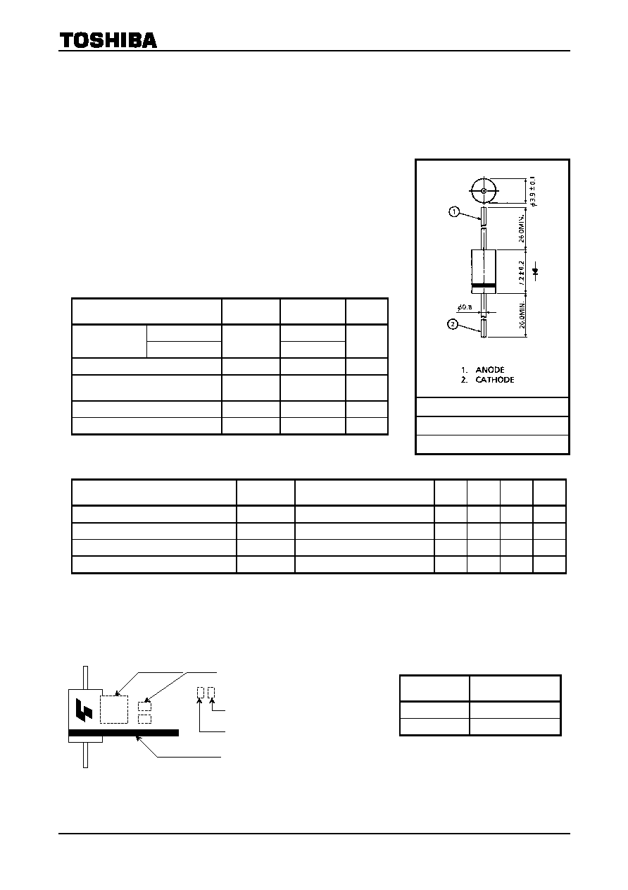
Note1: Soldering: 5 mm is the minimum to be kept between case and soldering part.
Note2: Lead bending: 5 mm is the minimum to be kept from the case when bend the lead wire.
Marking
Unit: mm
JEDEC
JEITA
TOSHIBA 3-4B1A
Weight: 0.47 g (typ.)
Type Code Lot No.
Cathode Mark
Color: Silver
Month (starting from alphabet A)
Year (last number of the christian era)
Code Type
VR4J TVR4J
VR4N TVR4N
V R
4 J

TVR4J,TVR4N
2002-09-18
2
30
0.4
2.0
0.6 0.8 1.0 1.2
1.6
Tj = 25∞C
150
0.2
10
5
3
1
0.5
1.4 1.8
0.01
10
1
0.1
0.0001
0.001
0.01
0.1 1 10 100
100
Ta
= 25∞C
100
0
80
60
40
20
Tj = 25∞C
f
= 50 Hz
1 3
5
10
30 100
160
0
120
60
40
20
0 0.2 0.4 0.6 0.8
80
100
140
Capacitive load
Sine wave
Solder
land
30
¥ 30 mm
Solder
land
20
¥ 20 mm
Solder
land
10
¥ 10 mm
Solder
land
less
full
lead
a
¥ a: solder land
5 mm
5 mm
a
a
a
a
5 mm
160
0
120
60
40
20
0
0.2
0.4
1.0 1.4
2.0
0.6
0.8
1.2 1.6
1.8
80
100
140
Solder
land
30
¥ 30 mm
Solder
land
20
¥ 20 mm
Solder
land
10
¥ 10 mm
Solder
land
less
full
lead
Resistive and
inductive load
a
¥ a: solder land
5 mm
5 mm
a
a
a
a
5 mm
5 mm
Sine wave
Instantaneous forward voltage v
F
(V)
i
F
≠ v
F
Instantan
eo
us f
o
rw
ar
d cu
rr
ent
i
F
(
A
)
Time t (s)
r
th (j-a)
≠ t
T
r
a
n
si
e
n
t t
h
e
r
m
a
l
i
m
pe
da
nce
r
th (j-a)
(∞C
/W
)
Number of cycles
Surge forward current (non-repetitive)
P
eak s
u
r
ge f
o
rw
ar
d c
u
rr
en
t
I
FSM
(A
)
Average forward current I
F (AV)
(A)
Ta max ≠ I
F (AV)
Maxi
mu
m al
l
o
w
a
bl
e
te
mpe
r
a
t
ur
e
T
a
m
a
x
(
∞
C
)
Average forward current I
F (AV)
(A)
Ta max ≠ I
F (AV)
Maxi
mu
m al
l
o
w
a
bl
e
te
mpe
r
a
t
ur
e
T
a
m
a
x
(
∞
C
)

TVR4J,TVR4N
2002-09-18
3
∑ TOSHIBA is continually working to improve the quality and reliability of its products. Nevertheless, semiconductor
devices in general can malfunction or fail due to their inherent electrical sensitivity and vulnerability to physical
stress. It is the responsibility of the buyer, when utilizing TOSHIBA products, to comply with the standards of
safety in making a safe design for the entire system, and to avoid situations in which a malfunction or failure of
such TOSHIBA products could cause loss of human life, bodily injury or damage to property.
In developing your designs, please ensure that TOSHIBA products are used within specified operating ranges as
set forth in the most recent TOSHIBA products specifications. Also, please keep in mind the precautions and
conditions set forth in the "Handling Guide for Semiconductor Devices," or "TOSHIBA Semiconductor Reliability
Handbook" etc..
∑ The TOSHIBA products listed in this document are intended for usage in general electronics applications
(computer, personal equipment, office equipment, measuring equipment, industrial robotics, domestic appliances,
etc.). These TOSHIBA products are neither intended nor warranted for usage in equipment that requires
extraordinarily high quality and/or reliability or a malfunction or failure of which may cause loss of human life or
bodily injury ("Unintended Usage"). Unintended Usage include atomic energy control instruments, airplane or
spaceship instruments, transportation instruments, traffic signal instruments, combustion control instruments,
medical instruments, all types of safety devices, etc.. Unintended Usage of TOSHIBA products listed in this
document shall be made at the customer's own risk.
∑ The information contained herein is presented only as a guide for the applications of our products. No
responsibility is assumed by TOSHIBA CORPORATION for any infringements of intellectual property or other
rights of the third parties which may result from its use. No license is granted by implication or otherwise under
any intellectual property or other rights of TOSHIBA CORPORATION or others.
∑ The information contained herein is subject to change without notice.
000707EAA
RESTRICTIONS ON PRODUCT USE