U30GWJ2C53C
2003-02-17
1
TOSHIBA Schottky Barrier Rectifier Stack Trench Schottky Barrier Type
U30GWJ2C53C
Switching Mode Power Supply Application
Converter&Chopper Application
∑ Repetitive peak reverse voltage: V
RRM
= 40 V
∑ Average output recified current: I
O
= 30 A
∑ Power surface mount device for thin flat package.
"TFP" (Toshiba package name)
Maximum Ratings
(Ta
=
=
=
=
25∞C)
Characteristics Symbol
Rating
Unit
Repetitive peak reverse voltage
V
RRM
40 V
Repetitive peak reverse surge voltage
(Note1)
V
RRSM
48 V
Average output recified current
I
O
30
A
300 (50 Hz)
Peak one cycle surge forward current
(non-repetitive, sine wave)
I
FSM
330 (60 Hz)
A
Junction temperature
T
j
-40 to 125
∞C
Storage temperature range
T
stg
-40 to 150
∞C
Note1: Pulse width (tw) <
= 500 ns, duty (tw/T) <= 1/25
Handling Precaution
Schottky barrier diodes are having large-reverse-current-leakage characteristic compare to other rectifier
products. This current leakage and not proper operating temperature or voltage may cause thermal runaway.
Please take forward and reverse loss into consideration when you design.
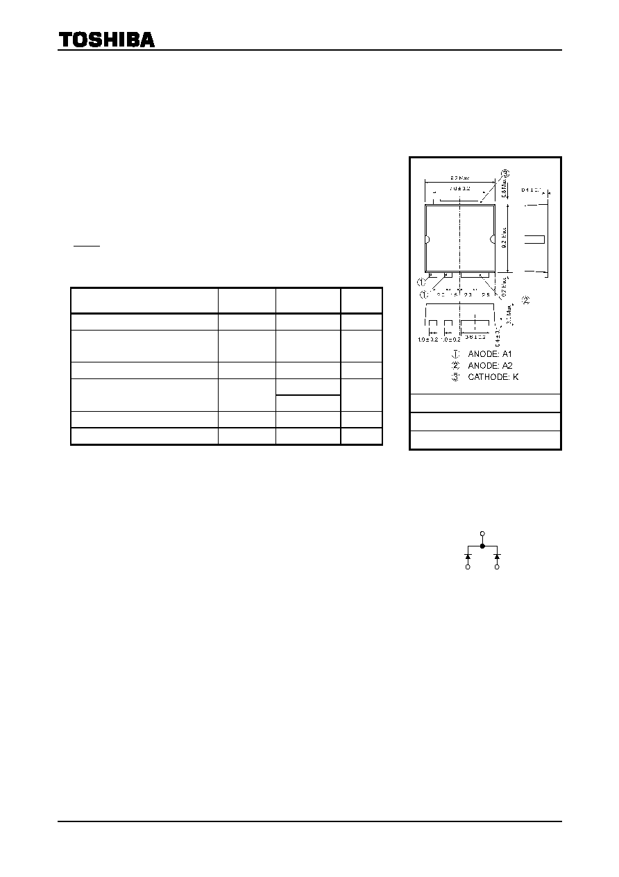
Unit: mm
JEDEC
JEITA
TOSHIBA 12-9B1A
Weight: 0.74 g (typ.)
Polarity
K
*A1 A2
*: Common Terminal

U30GWJ2C53C
2003-02-17
2
Electrical Characteristics
(Ta
=
=
=
=
25∞C)
Characteristics Symbol
Test
Condition
Min
Typ.
Max
Unit
Peak forward voltage
V
FM
I
FM
= 15 A
æ
æ 0.55
V
Repetitive peak reverse current
I
RRM
V
RRM
= 40 V
æ
æ 15 mA
Junction Capacitance
C
j
V
R
= 10 V, f = 1.0 MHz
æ 660 æ pF
Thermal resistance
R
th (j-c)
DC Total, Junction to Case
æ
æ 1.2
∞C/W
Note2: V
FM
, I
RRM
, C
j
: A value of one cell.
Marking
Standard Soldering Pad
2.5
2.
0
2.0
3.2
3.8
8.0
2.
0 6.
0
unit: mm
1 MARK
30GWJ2C
TYPE
U30GWJ2C53C
2 C
3
Lot Number
Month (starting from alphabet A)
Year (last number of the christian era)
3
1
2

U30GWJ2C53C
2003-02-17
3
i
F
≠ v
F
P
F (AV)
≠ I
o
Tc max ≠ I
o
r
th (j-c)
≠ t
C
j
≠ V
R
(typical)
T
r
a
n
si
e
n
t t
h
e
r
m
a
l
i
m
pe
da
nce
r
th (j-c)
(∞C
/
W
)
P
eak s
u
r
ge f
o
rw
ar
d c
u
rr
en
t
I
FSM
(A
)
Instantaneous forward voltage vF (V)
Instantan
eo
us f
o
rw
ar
d cu
rr
ent
i F
(A
)
Average output rectified current I
o
(A)
A
v
era
ge for
w
ar
d pow
er di
ssi
pati
on
P
F (A
V)
(W
)
Average output rectified current I
o
(A)
Maxi
mu
m al
l
o
w
a
bl
e
cas
e
te
mp
er
atu
r
e
T
c
m
a
x
(
∞
C)
Number of cycles
Time t (s)
Reverse voltage V
R
(V)
Juncti
on ca
p
a
ci
t
a
nce
C
j
(V
)
Surge forward current (non-repetitive)
0.1
0.001
10
1000
1
0.01 0.1 1 10 100
One cell
0
0
24
20
16
12
8
4
4 8
12 16 20
36
a = 30∞
60∞
90∞
120∞
180∞
sin
24 28 32
a 360∞
0∞
Conduction
angle
a
Rectangular
waveform
(one cell)
500
1 100
300
400
200
100
0
10
50 Hz
60 Hz
One cell
Single phase full
Sine wave
Ta
= 25∞C
10000
100
1 100
1000
10
f
= 1 MHz
Ta
= 25∞C
One cell
0.1
0.0
100
1
10
0.2 0.6
0.8
1.4
Tj
= 150∞C
100∞C
75∞C
25∞C
0.4
1.0 1.2
One cell
0
0
140
180∞
120∞
a = 30∞
60∞
90∞
120
100
80
60
40
20
36
32
28
4 20
24
sin
8 12 16
a 360∞
0∞
Conduction
angle
a
Rectangular
waveform
(one cell)

U30GWJ2C53C
2003-02-17
4
Junction temperature Tj (∞C)
I
R
≠ T
j
(typical)
Reve
r
s
e
cur
r
e
n
t I
R
(
m
A
)
Reverse voltage VR (V)
P
R (AV)
≠ V
R
(typical)
A
v
era
ge rev
e
rs
e pow
er di
ssi
pati
on
P
R
(A
V
) (W
)
3.0
0.0
0
2.0
1.0
20 40
30
10
60∞
120∞
180∞
240∞
300∞
DC
VR
Conduction
angle
a
Tj
= 150∞C
Rectangular
waveform
360∞
0∞
0.01
0
1000
0.1
10
50 100 150
1
20
VR = 10 V
30
25 75 125
100
40
Pulse measurement
(one cell)
U30GWJ2C53C
2003-02-17
5
∑ TOSHIBA is continually working to improve the quality and reliability of its products. Nevertheless, semiconductor
devices in general can malfunction or fail due to their inherent electrical sensitivity and vulnerability to physical
stress. It is the responsibility of the buyer, when utilizing TOSHIBA products, to comply with the standards of
safety in making a safe design for the entire system, and to avoid situations in which a malfunction or failure of
such TOSHIBA products could cause loss of human life, bodily injury or damage to property.
In developing your designs, please ensure that TOSHIBA products are used within specified operating ranges as
set forth in the most recent TOSHIBA products specifications. Also, please keep in mind the precautions and
conditions set forth in the "Handling Guide for Semiconductor Devices," or "TOSHIBA Semiconductor Reliability
Handbook" etc..
∑ The TOSHIBA products listed in this document are intended for usage in general electronics applications
(computer, personal equipment, office equipment, measuring equipment, industrial robotics, domestic appliances,
etc.). These TOSHIBA products are neither intended nor warranted for usage in equipment that requires
extraordinarily high quality and/or reliability or a malfunction or failure of which may cause loss of human life or
bodily injury ("Unintended Usage"). Unintended Usage include atomic energy control instruments, airplane or
spaceship instruments, transportation instruments, traffic signal instruments, combustion control instruments,
medical instruments, all types of safety devices, etc.. Unintended Usage of TOSHIBA products listed in this
document shall be made at the customer's own risk.
∑ The information contained herein is presented only as a guide for the applications of our products. No
responsibility is assumed by TOSHIBA CORPORATION for any infringements of intellectual property or other
rights of the third parties which may result from its use. No license is granted by implication or otherwise under
any intellectual property or other rights of TOSHIBA CORPORATION or others.
∑ The information contained herein is subject to change without notice.
000707EAA
RESTRICTIONS ON PRODUCT USE