 | –≠–ª–µ–∫—Ç—Ä–æ–Ω–Ω—ã–π –∫–æ–º–ø–æ–Ω–µ–Ω—Ç: VO4154H | –°–∫–∞—á–∞—Ç—å:  PDF PDF  ZIP ZIP |

VO4154/VO4156
Document Number 84797
Rev. 1.3, 08-Feb-06
Vishay Semiconductors
www.vishay.com
1
i179030
1
2
3
6
5
4
MT2
MT1
NC
A
C
NC
*Zero Crossing Circuit
ZCC*
Optocoupler, Phototriac Output, Zero Crossing, High dV/dt, Low
Input Current
Features
∑ High Static dV/dt 5 kV/µs
∑ High Input Sensitivity I
FT
= 1.6,
2.0, and 3.0 mA
∑ 300 mA On-State Current
∑ Zero Voltage Crossing Detector
∑ 400, and 600 V Blocking Voltage
∑ Isolation Test Voltage 5300 V
RMS
Agency Approvals
∑ UL1577, File No. E52744 System Code H or J,
Double Protection
∑ CUL -File No. E52744, equivalent to CSA bulletin
5A
∑ DIN EN 60747-5-2 (VDE 0884)
Available with Option 1
Applications
∑ Solid-state relays
∑ Industrial controls
∑ Office equipment
∑ Consumer appliances
Description
The VO4154/VO4156 consists of a GaAs IRLED opti-
cally coupled to a photosensitive zero crossing
TRIAC packaged in a DIP-6 package.
High input sensitivity is achieved by using an emitter
follower phototransistor and a cascaded SCR pre-
driver resulting in an LED trigger current of 1.6 mA for
bin D, 2.0 mA for bin H, and 3.0 mA for bin M.
The new phototriac zero crossing family uses a pro-
prietary dV/dt clamp resulting in a static dV/dt of
greater than 5 kV/µs.
The VO4154/VO4156 isolates low-voltage logic from
120, 240, and 380 VAC lines to control resistive,
inductive, or capacitive loads including motors, sole-
noids, high current thyristors or TRIAC and relays.
Order Information
For additional information on the available options refer to Option
Information.
Part
Remarks
VO4154D
400 V V
DRM
, I
ft
= 1.6 mA, DIP-6
VO4154D-X006
400 V V
DRM
, I
ft
= 1.6 mA, DIP-6 400 mil
VO4154D-X007
400 V V
DRM
, I
ft
= 1.6 mA, SMD-6
VO4154H
400 V V
DRM
, I
ft
= 2 mA, DIP-6
VO4154H-X006
400 V V
DRM
, I
ft
= 2 mA, DIP-6 400 mil
VO4154H-X007
400 V V
DRM
, I
ft
= 2 mA, SMD-6
VO4154M
400 V V
DRM
, I
ft
= 3 mA, DIP-6
VO4154M-X006
400 V V
DRM
, I
ft
= 3 mA, DIP-6 400 mil
VO4154M-X007
400 V V
DRM
, I
ft
= 3 mA, SMD-6
VO4156D
600 V V
DRM
, I
ft
= 1.6 mA, DIP-6
VO4156D-X006
600 V V
DRM
, I
ft
= 1.6 mA, DIP-6 400 mil
VO4156D-X007
600 V V
DRM
, I
ft
= 1.6 mA, SMD-6
VO4156H
600 V V
DRM
, I
ft
= 2 mA, DIP-6
VO4156H-X006
600 V V
DRM
, I
ft
= 2 mA, DIP-6 400 mil
VO4156H-X007
600 V V
DRM
, I
ft
= 2 mA, SMD-6
VO4156M
600 V V
DRM
, I
ft
= 3 mA, DIP-6
VO4156M-X006
600 V V
DRM
, I
ft
= 3 mA, DIP-6 400 mil
VO4156M-X007
600 V V
DRM
, I
ft
= 3 mA, SMD-6
e3

www.vishay.com
2
Document Number 84797
Rev. 1.3, 08-Feb-06
VO4154/VO4156
Vishay Semiconductors
Absolute Maximum Ratings
T
amb
= 25 ∞C, unless otherwise specified
Stresses in excess of the absolute Maximum Ratings can cause permanent damage to the device. Functional operation of the device is
not implied at these or any other conditions in excess of those given in the operational sections of this document. Exposure to absolute
Maximum Rating for extended periods of the time can adversely affect reliability.
Input
Output
Coupler
Parameter
Test condition
Symbol
Value
Unit
Reverse voltage
V
R
6.0
V
Forward current
I
F
60
mA
Surge current
I
FSM
2.5
A
Power dissipation
P
diss
100
mW
Derate from 25 ∞C
1.33
mW/∞C
Parameter
Test condition
Part
Symbol
Value
Unit
Peak off-state voltage
VO4154D/H/M
V
DRM
400
V
VO4156D/H/M
V
DRM
600
V
RMS on-state current
I
TM
300
mA
Total power dissipation
P
diss
500
mW
Derate from 25 ∞C
6.6
mW/∞C
Parameter
Test condition
Symbol
Value
Unit
Isolation test voltage (between
emitter and detector, climate per
DIN 500414, part 2, Nov. 74)
t = 1.0 min.
V
ISO
5300
V
RMS
Storage temperature range
T
stg
- 55 to + 150
∞C
Ambient temperature range
T
amb
- 55 to + 100
∞C
Soldering temperature
max.
10 sec. dip soldering
0.5 mm from case bottom
T
sld
260
∞C
Figure 1. Recommended Operating Condition
0
50
100
150
200
250
300
350
- 40 - 20
0
20
40
60
80
100
Temperature (∞C)
Load C
u
rrent (mA)
I
F
= 3 mA to 10 mA
19623
VO4154/VO4156
Document Number 84797
Rev. 1.3, 08-Feb-06
Vishay Semiconductors
www.vishay.com
3
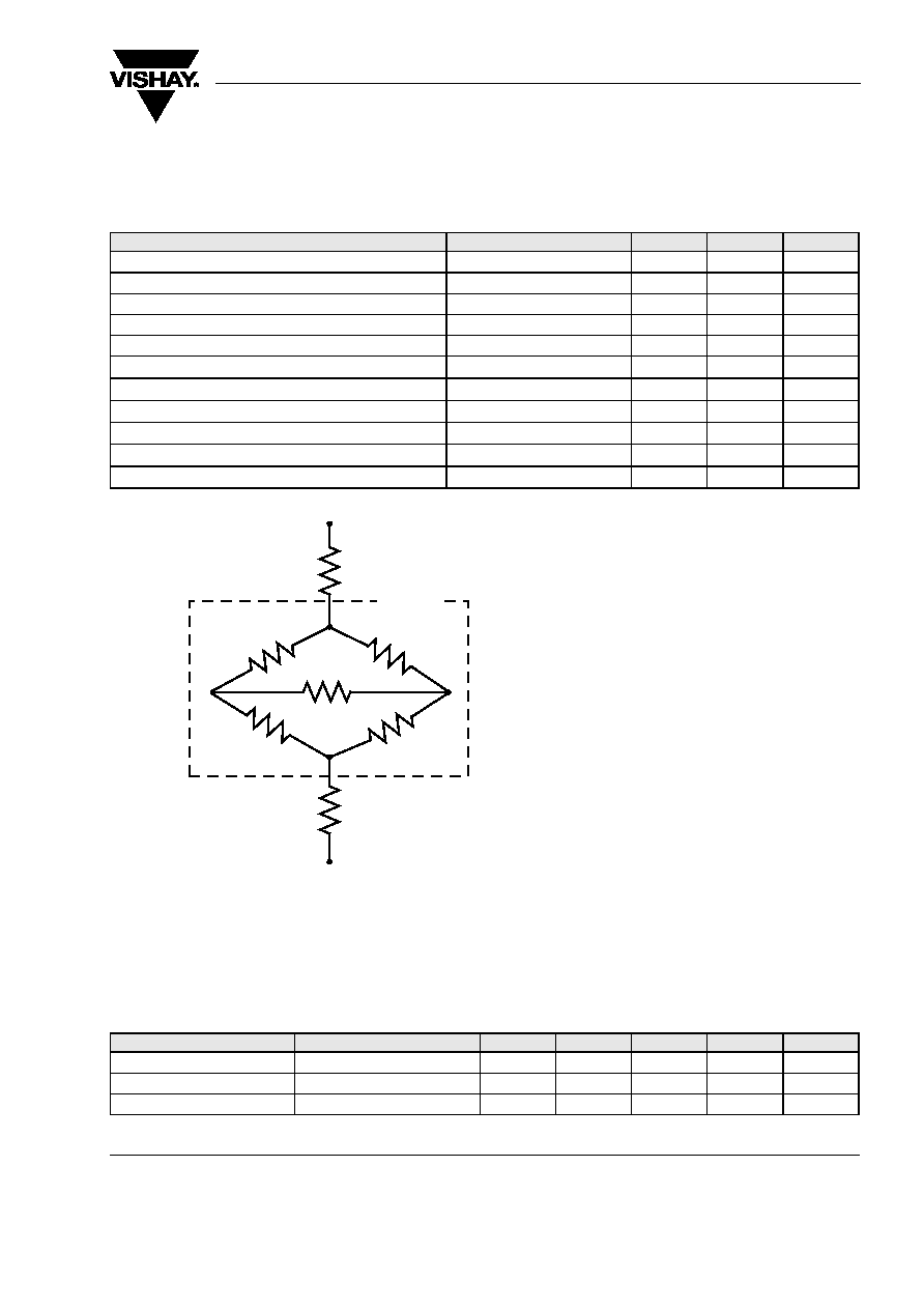
Thermal Characteristics
The thermal model is represented in the thermal network below. Each resistance value given in this model can be used to calculate the tem-
peratures at each node for a given operating condition. The thermal resistance from board to ambient will be dependent on the type of PCB,
layout and thickness of copper traces. For a detailed explanation of the thermal model, please reference Vishay's Thermal Characteristics
of Optocouplers Application note.
Electrical Characteristics
T
amb
= 25 ∞C, unless otherwise specified
Minimum and maximum values are testing requirements. Typical values are characteristics of the device and are the result of engineering
evaluation. Typical values are for information only and are not part of the testing requirements.
Input
Parameter
Test condition
Symbol
Value
Unit
LED Power dissipation
at 25 ∞C
P
diss
100
mW
Output Power dissipation
at 25 ∞C
P
diss
500
mW
Total Power dissipation
at 25 ∞C
P
tot
600
mW
Maximum LED junction temperature
T
jmax
125
∞C
Maximum output die junction temperature
T
jmax
125
∞C
Thermal resistance, Junction Emitter to Board
JEB
150
∞C/W
Thermal resistance, Junction Emitter to Case
JEC
139
∞C/W
Thermal resistance, Junction Detector to Board
JDB
78
∞C/W
Thermal resistance, Junction Detector to Case
JDC
103
∞C/W
Thermal resistance, Junction Emitter to Junction Detector
JED
496
∞C/W
Thermal resistance, Case to Ambient
CA
3563
∞C/W
T
A
CA
T
C
T
JD
T
JE
T
B
EC
EB
DC
DB
BA
DE
T
A
19996
Package
Parameter
Test condition
Symbol
Min
Typ.
Max
Unit
Forward voltage
I
F
= 10 mA
V
F
1.2
1.4
V
Reverse current
V
R
= 6.0 V
I
R
0.1
10
µA
Input capacitance
V
F
= 0 V, f = 1.0 MHz
C
I
25
pF

www.vishay.com
4
Document Number 84797
Rev. 1.3, 08-Feb-06
VO4154/VO4156
Vishay Semiconductors
Output
Coupler
Saftey and Insulation Ratings
Parameter
Test condition
Part
Symbol
Min
Typ.
Max
Unit
Repetitive peak off-state voltage
I
DRM
= 100 µA
VO4154D/H/M
V
DRM
400
V
VO4156D/H/M
V
DRM
600
V
Off-state current
V
D
= V
DRM
, I
F
= 0
I
DRM
100
µA
On-state voltage
I
T
= 300 mA
V
TM
3.0
V
On-state current
PF = 1.0, V
T(RMS)
= 1.7 V
I
TM
300
mA
Off-state current in inhibit state
I
F
= 2 mA, V
DRM
I
DINH
200
µA
Holding current
I
H
500
µA
Zero cross inhibit voltage
I
F
= Rated I
FT
V
IH
20
V
Critical rate of rise of off-state
voltage
V
D
= 0.67 V
DRM
, T
J
= 25 ∞C
dV/dt
cr
5000
V/µs
Critical rate of rise of on-state
dI/dt
cr
8.0
A/µs
Parameter
Test condition
Part
Symbol
Min
Typ.
Max
Unit
LED trigger current, current
required to latch output
V
D
= 3 V
VO4154D
I
FT
1.6
mA
VO4154H
I
FT
2.0
mA
VO4154M
I
FT
3.0
mA
VO4156D
I
FT
1.6
mA
VO4156H
I
FT
2.0
mA
VO4156M
I
FT
3.0
mA
Common mode coupling
capacitance
C
CM
0.01
pF
Capacitance (input-output)
f = 1.0 MHz, V
IO
= 0 V
C
IO
0.8
pF
Parameter
Test condition
Symbol
Min
Typ.
Max
Unit
Climatic Classification (according to IEC 68 part 1)
55/100/21
Polution Degree (DIN VDE 0109)
2.0
Comparative tracking index per DIN IEC 112/VDE
0303 part 1, group IIIa per DIN VDE 6110 175 399
175
399
V
IOTM
V
IOTM
8000
V
V
IORM
V
IORM
890
V
P
SO
P
SO
500
mW
I
SI
I
SI
250
mA
T
SI
T
SI
175
∞C
Creepage
7.0
mm
Clearance
7.0
mm

VO4154/VO4156
Document Number 84797
Rev. 1.3, 08-Feb-06
Vishay Semiconductors
www.vishay.com
5
Figure 2. Diode Forward Voltage vs. Forward Current
Figure 3. Diode Reverse Voltage vs. Temperature
Figure 4. Leakage Current vs. Ambient Temperature
0.7
0.9
1.1
1.3
1.5
0.1
1.0
10.0
I
F
(mA)
V
F
(
V
)
0 ∞C
25 ∞C
50 ∞C
19660
100.0
32
34
36
38
40
42
- 60 - 40 - 20
0
20
40
60
80
100
Temperature (∫C)
V
R
(
V
)
I
R
= 10 µA
19662
1
10
100
1000
10000
0
20
40
60
80
100
T
A
,Ambient Temperature (∞C)
I
DRM
, Leakage C
u
rrent (nA)
20008
I
RDM
at 630 V
Figure 5. On State Current vs. On State Voltage
Figure 6. Output Off Current (leakage) vs. Voltage
Figure 7. Normalize Trigger Input Current vs. Temperature
1
10
100
1000
1.0
1.5
2.0
2.5
3.0
3.5
25 ∞C
85 ∞C
0 ∞C
I
F
= 2 mA
V
TM
, On - State Voltage (V)
I
TM
, On - State C
u
rrent (mA)
19685
0
500
1000
1500
2000
2500
3000
3500
4000
4500
5000
0
200
400
600
800
Voltage (V)
O
u
tp
u
t Leakage c
u
rrent (nA)
85 ∞C
25 ∞C
0 ∞C
20009
0.0
0.2
0.4
0.6
0.8
1.0
1.2
1.4
1.6
1.8
- 60 - 40 - 20
0
20
40
60
80 100
Temperature (∫C)
N
ormalized I
FT
Normalized I
FT
at 25 ∫C
19666

www.vishay.com
6
Document Number 84797
Rev. 1.3, 08-Feb-06
VO4154/VO4156
Vishay Semiconductors
Figure 8. I
FT
(mA) vs. Turn-on time (µs)
Figure 9. Normalized Holding Current vs. Temperature
Figure 10. I
FT
vs. LED pulse width
0.0
0.5
1.0
1.5
2.0
2.5
3.0
3.5
10
100
1000
Turn-on time (µs)
I
FT
(mA)
20010
0.0
0.2
0.4
0.6
0.8
1.0
1.2
1.4
- 60 - 40 - 20
0
20
40
60
80 100
Temperature (∫C)
N
ormalized I
H
Normalized I
H
at 25 ∞C
20011
0
2
4
6
8
10
12
14
16
18
20
22
10
20
30
40
50
60
70
Trigger pulse width (µs)
I
FT
, Trigger c
u
rrent (mA)
85 ∫C
100 ∫C
25 ∫C
- 40 ∫C
20012

VO4154/VO4156
Document Number 84797
Rev. 1.3, 08-Feb-06
Vishay Semiconductors
www.vishay.com
7
Ozone Depleting Substances Policy
Statement
It is the policy of Vishay Semiconductor GmbH to
1. Meet all present and future national and international statutory requirements.
2. Regularly and continuously improve the performance of our products, processes, distribution and operating
systems with respect to their impact on the health and safety of our employees and the public, as well as
their impact on the environment.
It is particular concern to control or eliminate releases of those substances into the atmosphere which are
known as ozone depleting substances (ODSs).
The Montreal Protocol (1987) and its London Amendments (1990) intend to severely restrict the use of ODSs
and forbid their use within the next ten years. Various national and international initiatives are pressing for an
earlier ban on these substances.
Vishay Semiconductor GmbH has been able to use its policy of continuous improvements to eliminate the use
of ODSs listed in the following documents.
1. Annex A, B and list of transitional substances of the Montreal Protocol and the London Amendments
respectively
2. Class I and II ozone depleting substances in the Clean Air Act Amendments of 1990 by the Environmental
Protection Agency (EPA) in the USA
3. Council Decision 88/540/EEC and 91/690/EEC Annex A, B and C (transitional substances) respectively.
Vishay Semiconductor GmbH can certify that our semiconductors are not manufactured with ozone depleting
substances and do not contain such substances.
We reserve the right to make changes to improve technical design
and may do so without further notice.
Parameters can vary in different applications. All operating parameters must be validated for each
customer application by the customer. Should the buyer use Vishay Semiconductors products for any
unintended or unauthorized application, the buyer shall indemnify Vishay Semiconductors against all
claims, costs, damages, and expenses, arising out of, directly or indirectly, any claim of personal
damage, injury or death associated with such unintended or unauthorized use.
Vishay Semiconductor GmbH, P.O.B. 3535, D-74025 Heilbronn, Germany

Legal Disclaimer Notice
Vishay
Document Number: 91000
www.vishay.com
Revision: 08-Apr-05
1
Notice
Specifications of the products displayed herein are subject to change without notice. Vishay Intertechnology, Inc.,
or anyone on its behalf, assumes no responsibility or liability for any errors or inaccuracies.
Information contained herein is intended to provide a product description only. No license, express or implied, by
estoppel or otherwise, to any intellectual property rights is granted by this document. Except as provided in Vishay's
terms and conditions of sale for such products, Vishay assumes no liability whatsoever, and disclaims any express
or implied warranty, relating to sale and/or use of Vishay products including liability or warranties relating to fitness
for a particular purpose, merchantability, or infringement of any patent, copyright, or other intellectual property right.
The products shown herein are not designed for use in medical, life-saving, or life-sustaining applications.
Customers using or selling these products for use in such applications do so at their own risk and agree to fully
indemnify Vishay for any damages resulting from such improper use or sale.