
High Effiency DC /DC Converter
20 Watt TSI-20N Series
TSI-20N series is a small size (33◊21.5◊6mm size) and light weight ( g) step-down DC-DC converter with 20W.
Since it can operate from ultra low output voltage of 0.8V, it can be used for latest DSP, ASIC applications. High efficiency,
ulra high-speed response by synchronous rectification topology. No external components required.
Input: +3.3V/+5.0V Output: +1.8V, +2.0V, +2.5V, +3.3V (+0.8V ~ +3.6V)
Features
- High-speed response
- Non-Isolated Type Converter
- Ultra high Efficiency 93%
- Amazing Minimum Size
- ON/OFF Control
- Operating Temp. -40∞C~+85∞C
- Adjustable Output
- No Heat Sink required
- Latest Power-IC adopted
- High Reliability, High Performance
- Synchronous Rectification Circuit
- Additional external capacitor not required
- Short-Circuit, Over-Current Protection
Model
Standard Input Input Voltage
Output
Output
Non-Load
Ripple &
Efficiency
Package
Voltage
Range
Voltage
Current
Current
Noise
Vdc
Vdc~Vdc
Vdc
A
mA(typ)
mVpp(typ)
%(typ)
type
TSI 20N-0510V
SIP
TSI 20N-0510D
5.0
+3.0~5.5 (*1) +3.3(0.8~3.6)
6
3
40
93
DIP
TSI 20N-0510S
SMD
(*1) Input Voltage should be 0.5V or more higher than output voltage.
Specification
Standard Output Voltage When Vadj pin is open, output voltage will be set at +3.3V. (The accuracy of output V setting is ±3% max.)
Adjustable Output V Rang Output Voltage is adjustable according to the range above.
Line Reg.
0.7%typ. 1.5%max. (For the regulation of Input Voltage Range 3.8~5.5V)
Load Reg.
2.0%typ. 4.0%max. (For 0~6A of Load Reg., at Rating Input.
Temp. Coefficient
±0.02%/∞C typ. (For the change of Operating Temp. -10∞C~+50∞C)
Ripple & Noise
120mVpp max. (Rating Input, Rating Output, Room Temp.) (Measurements Frequency Band Width 20MHz)
Efficiency
93% (Rating Input/ Output, Room Temp., Refer Table 1)
Over-Current Protection
Operates at 105% or moreRating Load Current, auto recovery type. Avoid long time of short-circuit condition.
Over-Voltage Protection
None
Standby Current
2.4mA typ.
Remote
ON/OFF
Between 1pin(ON/OFF) 5~8pin(S.GND) [Open
: Output
ON, Short
: Output
OFF(Refer to application)]
Remote Sensing
The voltage between converter's output pin voltage between 7-8pin and sensing voltage difference
[voltage between 6-9pin] is 10% of sensing voltage (0.1V~0.3V) or below.
Operating Temp. Range
Operating Temp. -40∞C~+85∞C (Refer to the thermal derating graph.)
Storage Temp. Range
Storage Temp. -40∞C~+85∞C
Humidity Range
20%
~
95%R.Hmax. (Max. Wet-bulb Temp. 35∞C, non-condensing)
Cooling Condition
Refer to the thermal derating graph
Vibration
5~10Hz Every amplitude 10mm (3directions, each for 1hour), 10~55Hz acceleration 2G (3directions, each for 1hour)
Weight
4g typ.
External Dimensions
SIP type W=24 L=33 H=5.0 typ.
(
mm
)
(For dimensions refer to outline.)
DIP type W=22.25 L=33 H=6.0 typ.
(
mm
)
(For dimensions refer to outline.)
SMD type W=23.9 L=33 H=6.0 typ.
(
mm
)
(For dimensions refer to outline.)
* The above specification will be provided at rating value, when there is no specified condition described.
1
T e n t
a tiv e
T e n t
a tiv e

TSI 20N Series
1. TSI 20N-0510V (SIP type)
Pin
Function
1
on/off
2
Vin
3
Vin
4
Vin
5
GND
6
GND
7
GND
8
GND
9
Vout
- Dimensions: mm
10
Vout
- Dimension difference with
11
Vout
nothing specified ±0.5
12
V.ADJ
2. TSI 20N-0510D (DIP type)
Pin
Function
Pin
Function
1
on/off
11
Vout
2
Vin
12
V.ADJ
3
Vin
13
NC
4
Vin
14
+S
5
GND
15
-S
6
GND
22
NC
7
GND
23
P-Good
8
GND
24
NC
9
Vout
10
Vout
- Dimensions: mm
- Dimension difference with
nothing specified ±0.5
3. TSI 20N-0510S (SMD type)
Pin
Function
Pin
Function
1
on/off
11
Vout
2
Vin
12
V.ADJ
3
Vin
13
NC
4
Vin
14
+S
4
Vin
15
-S
5
GND
22
NC
6
GND
23
P-Good
7
GND
24
NC
8
GND
24
NC
8
GND
9
Vout
10
Vout
- Dimensions: mm
- Dimension difference with
nothing specified ±0.5
2
0.25
1.0typ
3.0typ
5.0m ax
0.8
33m a x
1
3.
5
±
1.
5
P2 .54◊11=27.94
0.5
12
21.
5(
+
1
,
-
0.
5)
24m
a
x
0.
25
22.
25±
0.
6
0.5
6.
0m
ax
3.
5±
1.
5
P2.54◊11=27.94
33m ax
1
C/L
21.
5(
+
1
,
-
0.
5)
12
13
24
23.
9
±
0.
8
0.5
6.
0m
ax
P2.54◊11=27.94
33m ax
1
C/L
21.
5(
+
1
,
-
0.
5
)
12
13
24
A
Detailed figure of
com ponent
A
0
~
10∞
(1.2)
0.
25
T e n t
a tiv e
T e n t
a tiv e
Standard Connection Circuit Diagram
Figure 6
Note 1: When not using the ON/OFF control, keep ON/OFF pin open.
Note 2: When not adjusting output, keep V.ADJ pin open.
Note 3: When it includes inductance in input line or switch ing element is connected to the input side or the wire is long,
to fulfill the performance C1 will be required. Also to lower the input impedance we recommend a pattern that has an
additional C1, and to verify on a actual equipment. Or, by adding C2 you can lower the output ripple more.
Recommended Capacitor
C1=33 µF10WV
C2=2.2 µF~22µF
C2: An output capacitor is built-in so it is not required, however by connecting 2.2 µF~22 µF you can lower the noise more
Note 4: There is no +S, Pin in TSI 20N-0510V SIP type.
Method of Adjusting Output Voltage
When using at 3.3V without adjusting output voltage, keep V.ADJ pin (12Pin) open.
By connecting a resistor between +Vout pin (9~11Pin)~V.ADJ pin (12Pin), you can adjust the output voltage in the range of 0.8~3.3V.
(Vout Down Control)
By connecting a resistor between Vadj pin (12Pin)~GND pin (5~8Pin), you can adjust the output voltage in the range of 3.3V~3.6V.
(Vout Up Control)
To calculate external resistance, please refer to the equation below. After calculating external resistance, please check output voltage
and adjust resistance value.
To set in the range of 0.8V~3.3V
To set in the range of 3.3V~3.6V
Vo= Requested output V Adjustable voltage range=0.8~3.6V
Rx=10.2k ohm
Ry=2.7k ohm
Rz=0.1K ohm
Figure 7
Vs=0.703V
3
TSI 20N Series
V in
C 1
o n /o ff
V in
V o u t
V a d j
L o a d
V o u t
B S V
S e rie s
G N D
S W
O p e n = O n
S h o rt= O ff
R 1 :V o u t D o w n s etted res isto r
R 2 :V o u t U P se tte d re sis to r
+ S
-S
R 1
C 2
R 2
R x
V s
R y
V .A D J
+V ou t
R 1
B S V
S eries
9,10 ,1 1
12
5,6,7,8
Lo ad
G N D
R z
R 2
Rx ◊ Ry (Vo-Vs)
Rx ◊ Vs-Ry (Vo-Vs)
R1=
R2=
Rx ◊ Ry ◊ Vs
Ry (Vo-Vs) -Rx ◊ Vs
-Rz
-Rz
T e n t
a tiv e
T e n t
a tiv e
TSI20N
Series

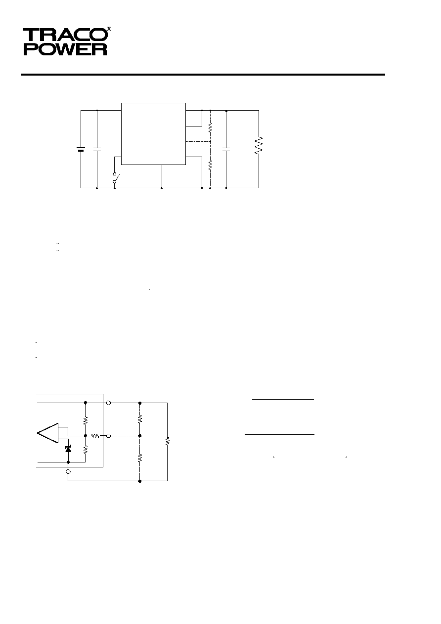
Remote ON/OFF Control
- ON/OFF Function
By using this ON/OFF control function, the output can be ON/OFF controlled without intermitting input.
This is an effective function when composing a power supply system sequence. And this can also be used as a power standby function for
saving power control.
- Not using ON/OFF Function
To not use the ON/OFF function, keep ON/OFF pin open.
- Method of ON/OFF Control
Between ON/OFF pin
(
1Pin
) and
S.GND
(5~8
Pin
)
Open ---- Output=ON
Short ---- Output=OFF (0~0.7V 1∑A max.)
To prevent reverse connection of Input Power Supply (ex.)
This prodcut is a non-isolated type DC-DC converter that steps-down
from (+) to (+).
If you connect the input voltage reversed by mistake,
it will be damaged.
If there is a possibility of reverse connection, please
add a protection as the right figure.
The right figure is an example using huse and diode.
Over-Voltage Protection (ex.)
This product does not have a built-in over-voltage protection.
If the switching element in this converter is damaged in short mode
input voltage +Vin will be output as is.
However, to prepare for damage at over-voltage mode, we recommend to
add a circuit to intercept the supplying power circuit.
Note1: When it is damaged at over-voltage mode, ON/OFF control does
not operate.
Note2: When there is a ON/OFF function on the supplying power side,
this may be used.
Note 3: Be sure that the DC power supply on the supplying side has
the capacity to fuse the fuse.
Soldering Conditions
Solder under the following conditions.
1. With soldering iron
340∞C~360∞C within 3sec.
2. With soldering dip
240∞C~260∞C within 10sec.
3. Reflow method (only for SMD type)
Preheating Temp.: 150±10∞C, within 1min.
Main heating temp.: 235∞Cmax. 10sec max.
Reflowing frequency: once
4
TSI 20N Series
5 ,6 ,7 ,8
1
B SV
S eries
o r
E xam p le
o n /o ff
G N D
2,3,4
1
9,10,11
+V out
5,6,7,8
F U S E
+V in
V .A D J
on/off
12
G N D
D 1
+ Vin
Load
B S V
S eries
L oa d
2 ,3 ,4
1
9 ,1 0,11
+V out
5 ,6 ,7 ,8
B S V
S eries
FU S E
+V in
V .A D J
o n/off
1 2
G N D
O ver-
V oltage
detec tion
circuit
+ V in
S C R
M ain
heating
T im e
Te
m
p
.
P reheating
T e n
ta tiv
e
T e n
ta tiv
e
TSI20N
Series
TSI20N
Series
TSI20N
Series

TSI 20N Series
Block Diagram
* There is no P-Good, +S, -S pin inTSI 20-0510S (SIP type).
Thermal Derating
Please set this product in a place with good circulation.
And when using this product in an environment that ambient temp. is 40∞C or more, please refer to the thermal derating below.
5
C 1
C 2
R z
R y
R x
L 1
P O W E R
@
IC
V in
4
G N D
6
O N /O F F
1
V in
3
V o u t
1 1
V o u t
9
V o u t
1 0
G N D
7
G N D
6
+ S
1 4
-S
1 5
V .A D J
1 2
P - G o o d
2 3
V in
2
G N D
5
VF
B
-
VF
B
+
ON
/OF
F
P-
Go
od
c o n tr o l
A m bien t T e m p. (∞C )
Lo
ad
C
u
r
r
en
t
D
e
r
a
t
i
ng
r
a
t
e
(
%
)
-10
0
1 0
2 0
3 0
4 0
5 0
6 0
7 0
8 0 8 5
0
1 0
2 0
3 0
4 0
5 0
6 0
7 0
8 0
9 0
0 m/s
1 .5m /s
0 .5m /s
-20
-30
-40
1 00