 | –≠–ª–µ–∫—Ç—Ä–æ–Ω–Ω—ã–π –∫–æ–º–ø–æ–Ω–µ–Ω—Ç: EB-TA0102 | –°–∫–∞—á–∞—Ç—å:  PDF PDF  ZIP ZIP |
T E C H N I C A L I N F O R M A T I O N
EB-TA0102 01.01, Rev. 3.3
1
CLASS-T DIGITAL AUDIO AMPLIFIER EVALUATION BOARD USING
DIGITAL POWER PROCESSING
TM
TECHNOLOGY
EB-TA0102
January 2001, For Rev. 3.3 Board
General Description
The EB-TA0102 evaluation board is based on the TA0102A digital audio power amplifier from Tripath
Technology. This board is designed to provide a simple and straightforward environment for the
evaluation of the Tripath stereo TA0102A amplifier. This board can also be used in a bridged
configuration for high power mono output.
Features
ÿ
2 x 150W @ 0.1% THD+N, 4
ÿ
300W bridgeable subwoofer output, @
0.1% THD+N, 4
ÿ
Four N-Channel power MOSFETs
ÿ
Outputs short circuit protected
Benefits
ÿ
Quick, easy evaluation and testing of the
TA0102A amplifier
ÿ
Ready to use in many applications:
ÿ
2 channel stereo systems
ÿ
Powered 2.1 speaker systems
Powered Subwoofers
2

T E C H N I C A L I N F O R M A T I O N
EB-TA0102 01.01, Rev. 3.3 2
OPERATING INSTRUCTIONS
Power Supply Description
There are three external power supplies required to operate this board: Vspos, Vsneg and +5V (see
Figure 1). Vspos and Vsneg power the load and so must each be able to provide half of the desired
output power, plus about 20% for overhead and margin. The TA0102A amplifier also requires a supply,
VN12, that is 12V more positive than Vsneg and tracks Vneg. This evaluation board generates this
VN12 voltage on-board. All input, output and power supply connections are made using tinned wire or
female banana connectors (not shown).
Though not required, the following powering-up sequence is usually adhered to during bench
evaluations: 1
st
) +5V, 2
nd
) Vsneg and 3
rd
) Vspos (refer to the Turn-on/off Pop section). The positive and
negative supply voltages do not have to match or track each other, but distortion or clipping levels will be
determined by the lowest (absolute) supply voltage. For applications where VN12 is supplied
separately, make sure this supply tracks the Vsneg as it becomes more negative with respect to ground.
Once power is applied to the evaluation board, the green power light, LED 1, will illuminate. If it does
not, power the unit down and recheck all connections and supplies. If the MUTE jumper is missing, the
LED will not illuminate. To un-mute, short pins 2 and 3 of JP5. Please note that until the Vspos and
Vsneg have powered up and are within the undervoltage and overvoltage limits, the LED will be
illuminated (assuming everything else is properly connected). Once the amplifier is switching, if the
undervoltage or overvoltage limit is violated, LED 1 will turn off until supply voltages are within
specification.
Input Connections
Audio input to the board is located at IN1 and IN2 (see Figures 1 and 2). The input can be a test signal
or music source. Connections are made using tinned wired to IN1, IN2 and Analog Ground, AGND.
These connections are made on the evaluation board using a cable harness with female banana
connectors (not shown).
Output Connections
There are four female banana connectors on the evaluation board for speaker outputs OUT1, OUT2,
and Power Grounds, GND1 and GND2 (see Figures 1 and 2; cable harness connections are not shown).
The TA0102A can be operated as a two channel single-ended amplifier, bridged mono output amplifier
(see Figure 8) or with a passive crossover for a 2.1 channel application (refer to Application Note 13).
Outputs can be any passive speaker(s) or test measurement equipment (see Application Note 4
"Parametric Measurements" for more information on bench testing).
Note:
To avoid performance degradation, the Analog Ground and Power Grounds should be kept
separate. They are internally connected in the TA0102A amplifier.
T E C H N I C A L I N F O R M A T I O N
EB-TA0102 01.01, Rev. 3.3 3
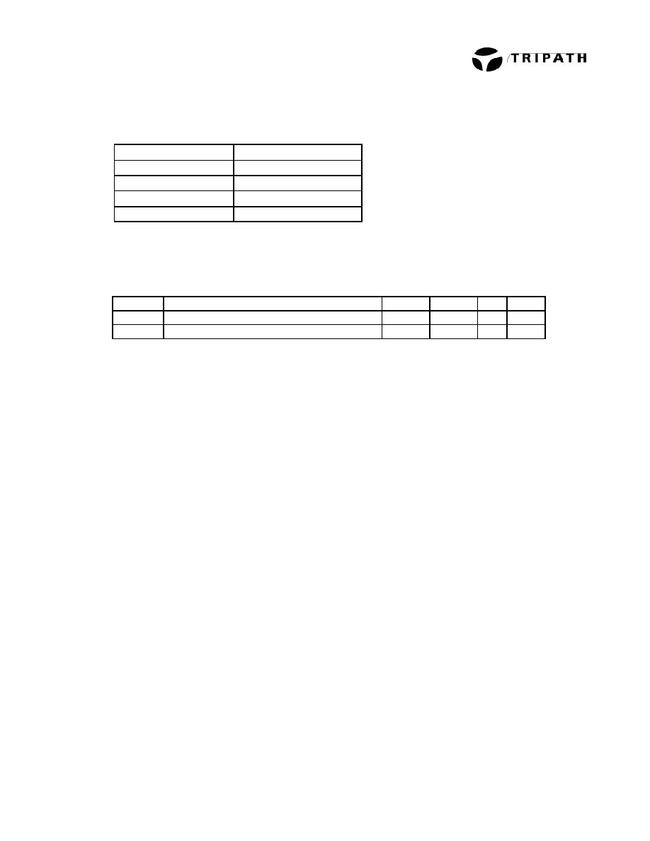
Connector Name
Channel
IN1
Channel 1 Input
IN2
Channel 2 Input
OUT1
Channel 1 Output
OUT2
Channel 2 Output
Board Operating Conditions
SYMBOL
PARAMETER
MIN.
TYP.
MAX. UNITS
V
S
Supply Voltage (V
spos
& V
sneg
)
+/-28
+/-49
V
V5
Positive 5V Bias Supply
4.5
5
5.5
V
See TA0102A data sheet for additional information on Absolute Maximum Ratings, Operating
Conditions, Electrical Characteristics and Performance Characteristics.
Turn-on/off Pop
To avoid turn-on pops, bring the mute from a high to a low state after all power supplies have settled. To
avoid turn-off pops, bring the mute from a low to a high state before turning off the supplies. The only
issue with bringing up the 5V last or turning it off first is clicks/pops. If the mute line is properly toggled
(slow turn-on, quick turn-off), then any power up sequence is fine. In practice, the 5V will usually
collapse before Vspos and Vsneg. This is acceptable and will not cause any damage to the TA0102A.

T E C H N I C A L I N F O R M A T I O N
4 EB-TA0102 01.01, Rev. 3.3
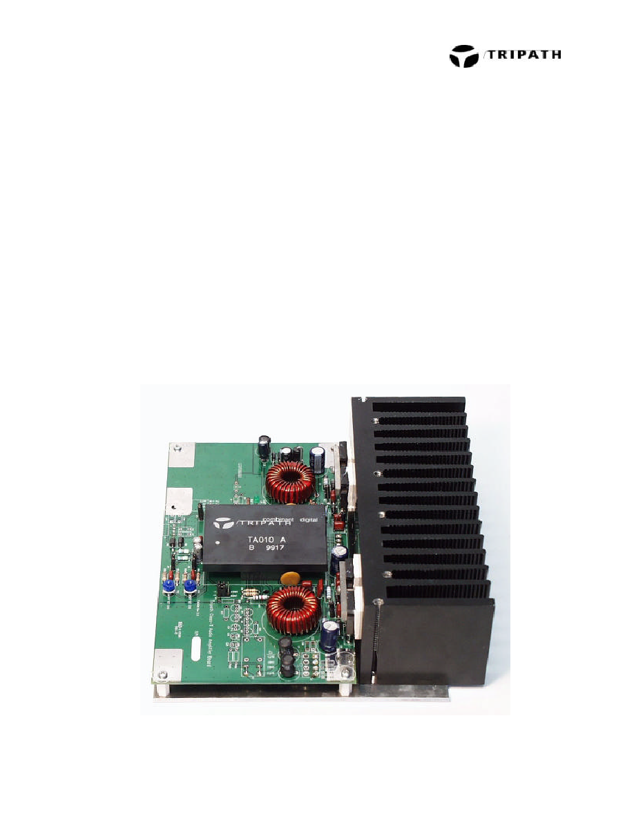
EB-TA0102 Board
Figure 1
*Please note the Break-Before-Make labels on the PC Board are incorrect and are reversed.
Figure 2
Output Transistors
Output Transistors
CONNECTIONS
Vspos (+V)
+5V
AGND
DGND
NC
Vsneg (-V)
Output
Connections
Input
Connections
Mute
Jumper
Power
LED
Voltage Offset
Adjust
Break Before
Make Jumpers
2
TA0102A
BBM0 BBM1
+
+
+V
+5
AG
DG
-V
NC
HEATSINK
MUTE
AGND
IN1
IN2
OUT1
GND1
GND2
OUT2
Tripath Class-T Audio
Amplifier Board
EB-TA0102, Rev. 3.3
LED
OFFSET CH1
OFFSET CH2
MUTE
N-Channel
MOSFETs, M1-M4
M1
M2
M3
M4

T E C H N I C A L I N F O R M A T I O N
EB-TA0102 01.01, Rev. 3.3 5
ARCHITECTURE
A block diagram of one channel of the evaluation board is shown in Figure 3. The major functional
blocks of the amplifier are described below.
Figure 3
Input Stage
Figure 4 shows one channel of the Input Stage. The TA0102A amplifier is designed to accept
unbalanced inputs and provide an overall gain of 7.05, or approximately 17 dB. Please note that the
input stage of the TA0102A is biased at approximately 2.5VDC. Therefore, for an input signal centered
around ground (0VDC), the polarity of the coupling capacitor, C
IN
, shown in Figure 4 is correct.
Figure 4
TA0102A
Output
Section
VN12
Out
Input Stage
In
+5V
1M
10K
0.1uF, 50V
1M
49.9K
1uF, 6.3V
Input to TA0102A
R
IN
C
IN
+
(DC Bias ~2.5V)