 | –≠–ª–µ–∫—Ç—Ä–æ–Ω–Ω—ã–π –∫–æ–º–ø–æ–Ω–µ–Ω—Ç: TA0104A | –°–∫–∞—á–∞—Ç—å:  PDF PDF  ZIP ZIP |

T r i p a t h T e c h n o l o g y, I n c . - T e c h n i c a l I n f o r m a t i o n
TA0104A
STEREO 500W (4
) CLASS-T DIGITAL AUDIO AMPLIFIER
DRIVER USING DIGITAL POWER PROCESSING (DPP
T M
)
TECHNOLOGY
T e c h n i c a l I n f o r m a t i o n
R e v i s i o n 3 . 1 ≠ J u n e 2 0 0 0
G E N E R A L D E S C R I P T I O N
T h e T A 0 1 0 4 A i s a 5 0 0 W c o n t i n u o u s a v e r a g e ( 4
) , t w o c h a n n e l A m p l i f i e r D r i v e r
M o d u l e w h i c h u s e s T r i p a t h ' s p r o p r i e t a r y D i g i t a l P o w e r P r o c e s s i n g ( D P P
T M
)
t e c h n o l o g y . C l a s s - T a m p l i f i e r s o f f e r b o t h t h e a u d i o f i d e l i t y o f C l a s s - A B a n d t h e
p o w e r e f f i c i e n c y o f C l a s s - D a m p l i f i e r s .
A P P L I C A T I O N S
Audio/Video
Amplifiers/Receivers
Pro-audio Amplifiers
Automobile Power Amplifiers
Subwoofer Amplifiers
B E N E F I T S
Reduced system cost with smaller/less
expensive power supply and heat sink
Signal fidelity equal to high quality Class-AB
amplifiers
High dynamic range compatible with digital
media such as CD and DVD
Features
Class-T architecture
Proprietary Digital Power Processing
technology
Supports wide range of output power levels
"Audiophile" Sound Quality
0.02% THD+N @ 300W, 8
0.02% IHF-IM @ 100W, 8
350W @ 8
, 0.1% THD+N,
Vs = +90V
500W @ 4
, 0.1% THD+N,
Vs = +90V
High Power
450W @ 8
, 1% THD+N,
Vs = +90V
750W @ 4
, 1% THD+N,
Vs = +90V
High Efficiency
90% @ 400W @ 8
,
Vs = +75V
85% @ 600W @ 4
, Vs = +75V
Dynamic Range = 106 dB
Requires only N-Channel MOSFET output transistors
High power supply rejection ratio
Mute input
Outputs short-circuit protected
Over- and under-voltage protection
Bridgeable, single-ended outputs
38-pin quad package
Supports 100kHz BW of Super Audio CD and DVD-
Audio (Refer to Application Note for specifics)
TYPICAL PERFORMANCE AT +90V
THD+N vs Output Power
T
HD+N (%)
Output Power (W)
0.01
10
0.02
0.05
0.1
0.2
0.5
1
2
5
0.005
0.001
0.002
20Hz - 22kHz BW
f = 1kHz
BBM = 25nS
V
S
= +/-90V
Av = 200
ST STW38NB20 MOSFET
R
L
= 4
R
L
= 8
1
500
2
5
10
20
50
100
200
1K
1
TA104A ≠ Rev. 3.1/06.00

T r i p a t h T e c h n o l o g y, I n c . - T e c h n i c a l I n f o r m a t i o n
Absolute Maximum Ratings
SYMBOL
PARAMETER
Value
UNITS
Vs
Supply Voltage (Vspos & Vsneg)
+/-100
V
V5
Positive 5 V Bias Supply
6
V
VN12
Reference Voltage: Nominal +12V referenced to Vsneg
18
V
T
STORE
Storage Temperature Range
-40 to 150
∫C
T
A
Operating Free-air Temperature Range
-20 to +80
∫C
Notes:
Absolute Maximum Ratings indicate limits beyond which damage to the device may occur.
Damage will occur to the device if VN12 is not supplied or falls below the recommended
operating voltage when V
S
is within its recommended operating range.
Operating Conditions
SYMBOL PARAMETER MIN.
TYP.
MAX.
UNITS
Vs
Supply Voltage (Vspos & Vsneg)
+/- 55 +/- 75 +/- 92
V
V5
Positive 5 V Bias Supply
4.5
5
5.5
V
VN12
Reference Voltage: Nominal +12V referenced to Vsneg
10.8
12
13.2
V
Note: Recommended Operating Conditions indicate conditions for which the device is functional. See Electrical
Characteristics for guaranteed specific performance limits.
Electrical Characteristics
T
A
= 25
∞C. See Notes 1 & 2 for Operating Conditions and Test/Application Circuit Setup.
SYMBOL PARAMETER
MIN.
TYP.
MAX.
UNITS
I
q
Quiescent Current
+67V
(no load, BBM0=BBM1=0)
-67V
+5V
VN12
50
50
45
170
mA
mA
mA
mA
I
S
Source Current @ P
OUT
= 250W, R
L
= 4
V
SPOS
= +67V
@ 10% THD+N
V
SNEG
= -67V
4.2
4.2
A
A
I5
Source Current for 5V Bias Supply @ P
OUT
= 250W, R
L
= 4
50
mA
IVN12
Source Current for VN12 Supply @ P
OUT
= 250W, R
L
= 4
80
mA
Vu
Under Voltage (Vspos & Vsneg)
+/-55
V
Vo
Over Voltage (Vspos & Vsneg)
+/-92
V
V
IH
High-level Input Voltage (MUTE)
3.5
V
V
IL
Low-level Input Voltage (MUTE)
1
V
I
DD
MUTE
Mute Supply Current
+67V
(no load, BBM0=BBM1=0)
-67V
+5V
VN12
0
0
15
0
mA
mA
mA
mA
V
OH
High-level Output Voltage (HMUTE & OVERLOADB)
3.5
V
V
OL
Low-level Output Voltage (HMUTE & OVERLOADB)
1
V
V
TOC
Over Current Sense Voltage Threshold
0.67
0.75
0.82
V
A
V
Gain Ratio V
OUT
/V
IN
, R
IN
= 0
160
V/V
Voffset
Offset Voltage, no load, MUTE = Logic low
600
mV
Minimum and maximum limits are guaranteed but may not be 100% tested.
2
TA104A ≠ Rev. 3.1/06.00

T r i p a t h T e c h n o l o g y, I n c . - T e c h n i c a l I n f o r m a t i o n
Performance Characteristics ≠ Single Ended, Vs = +90V
Unless otherwise specified, f = 1kHz, Measurement Bandwidth = 22kHz. T
A
= 25
∞C.
See Notes 1 & 2 for Operating Conditions and Test/Application Circuit Setup.
SYMBOL PARAMETER
CONDITIONS
MIN.
TYP.
MAX.
UNITS
P
OUT
Output
Pow er
(Continuous Average/Channel)
THD+N = 0.1%, R
L
= 8
R
L
= 4
THD+N = 1%,
R
L
= 8
R
L
= 4
350
500
450
750
W
W
W
W
THD + N
Total Harmonic Distortion Plus
Noise
P
OUT
= 300W/Channel, R
L
= 8
0.02
%
IHF-IM
IHF Intermodulation Distortion
19kHz, 20kHz, 1:1 (IHF), R
L
= 8
P
OUT
= 100W/Channel
0.02 %
SNR
Signal-to-Noise Ratio
A Weighted, P
OUT
= 350W/Ch, R
L
= 8 100.5 dB
CS
Channel Separation
0dBr = 100W, R
L
= 8
85
dB
PSRR
Pow er Supply Rejection Ratio
Input Referenced, 30kHz Bandw idth
65
dB
e
NOUT
Output Noise Voltage
A Weighted, no signal, input shorted, DC
offset nulled to zero
500 µV
Performance Characteristics ≠ Single Ended, Vs = +75V
Unless otherwise specified, f = 1kHz, Measurement Bandwidth = 22kHz. T
A
= 25
∞C.
See Notes 1 & 2 for Operating Conditions and Test/Application Circuit Setup.
SYMBOL PARAMETER
CONDITIONS
MIN.
TYP.
MAX.
UNITS
P
OUT
Output
Pow er
(Continuous Average/Channel)
THD+N = 0.1%, R
L
= 8
R
L
= 4
THD+N = 1%,
R
L
= 8
R
L
= 4
200
425
300
500
W
W
W
W
THD + N
Total Harmonic Distortion Plus
Noise
P
OUT
= 300W/Channel, R
L
= 4
0.02
%
IHF-IM
IHF Intermodulation Distortion
19kHz, 20kHz, 1:1 (IHF), R
L
= 8
P
OUT
= 100W/Channel
0.02 %
SNR
Signal-to-Noise Ratio
A Weighted, P
OUT
= 200W/Ch, R
L
= 8 98 dB
CS
Channel Separation
0dBr = 100W, R
L
= 8, f = 1kHz
85
dB
PSRR
Pow er Supply Rejection Ratio
Input Referenced, 30kHz Bandw idth
65
dB
Pow er
Efficiency
P
OUT
= 400W/Channel, R
L
= 8
90
%
e
NOUT
Output Noise Voltage
A Weighted, no signal, input shorted, DC
offset nulled to zero
500 µV
Minimum and maximum limits are guaranteed but may not be 100% tested.
Notes:
1) V5 = +5V, VN12 = +12V referenced to V
SNEG
2) Test/Application Circuit Values:
D = MUR120T3 diodes, R
IN
= 22.1K
R
D
= 33
, R
S
= 0.025
,R
G
= 5.6
R
OCR1
= R
OCR2
= 0
, L
F
= 18uH (Amidon core T200-2)
C
F
= 0.22uF, C
D
= 0.1uF, C
IN
= 1uF, C
BY
= 0.1uF
Power Output MOSFETs, M = ST STW38NB20
BBMO=BBM1=1
3
TA104A ≠ Rev. 3.1/06.00
T r i p a t h T e c h n o l o g y, I n c . - T e c h n i c a l I n f o r m a t i o n
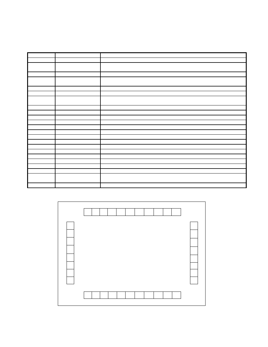
Pin Description
Pin
Function
Description
1 AGND
Analog
Ground
2
OVERLOADB
Logic output. When low, indicates that the level of the input signal has
overloaded the amplifier.
3
V5
Positive 5 Volts
4
MUTE
Logic input. When high, both amplifiers are muted. When low (grounded), both
amplifiers are fully operational.
5, 6
IN2, IN1
Single-ended input (Channel 1 & 2)
7, 8
BBM0, BBM1
Break-before-make timing control
9, 12
GNDKELVIN1,
GNDKELVIN2
Kelvin connection to speaker ground (Channel 1 & 2)
10, 11
OCR2, OCR1
Over-current threshold adjustment (Channel 1 & 2)
13, 14
OCS1L+, OCS1L-
Over Current Sense resistor, Channel 1 low-side
15, 16
OCS1H-, OCS1H+
Over Current Sense resistor, Channel 1 high-side
17, 30
LO1COM, LO2COM
Kelvin connection to source of low-side transistor (Channel 1 & 2)
18, 29
FDBKN1;FDBKN2
Feedback (Channel 1 & 2)
19
VN12
Voltage: +12 V from V
SNEG
. Refer to Application Information section.
20, 27
LO1, LO2
Low side gate drive output (Channel 1 & 2)
21, 26
HO1COM, HO2COM Kelvin connection to source of high-side transistor (Channel 1 & 2)
22, 25
HO1, HO2
High side gate drive output (Channel 1 & 2)
23 V
SPOS
Positive supply voltage
24 V
SNEG
Negative supply voltage
28 PGND
Power
Ground
31, 32
OCS2L-, OCS2L+
Over Current Sense resistor, Channel 2 low-side
33, 34
OCS2H-, OCS2H+
Over Current Sense resistor, Channel 2 high-side
35
HMUTE
Logic output. When high, indicates that the output stages of both amplifiers
are shut off and muted.
36, 37, 38
NC
Not Connected - Must Be Left Floating
38 Pin Quad Package Pin-out (Top View)
9
10
11
12
13
14
15
16
17
18
19
1
2
3
4
5
6
7
8
AGND
OVERLOADB
V5
IN2
IN1
BBM0
BBM1
MUTE
38
37
36
35
34
33
32
31
30
29
28
27
26
25
24
23
22
21
20
LO2
HO2COM
HO2
V
SNEG
V
SPOS
HO1
H01COM
LO1
GN
D
KELVIN
1
O
CR2
O
CR1
GN
D
KELVIN
2
OC
S1L+
OC
S1L-
OC
S1H
-
OC
S1H
+
LO1C
OM
FD
BKN
1
VN
12
NC
NC
NC
HMUTE
OC
S2H
+
OC
S2H
-
OC
S2L+
OC
S2L-
LO2C
OM
FD
BKN
2
PGN
D
4
TA104A ≠ Rev. 3.1/06.00
T r i p a t h T e c h n o l o g y, I n c . - T e c h n i c a l I n f o r m a t i o n
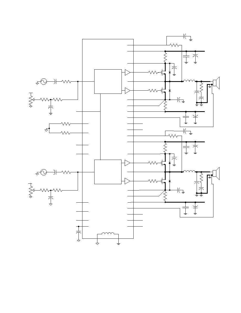
Test/Application Circuit
Processing
&
Modulation
TA0104A
MUTE
OVERLOADB
IN1
IN2
PGnd
AGnd
R
IN
R
IN
OCS1H-
HO1
HO1COM
OCS1L+
OCR1
OCR2
FDBKN1
VN12
R
S
V
SPOS
M
R
OCR1
R
OCR2
BBM0
BBM1
R
L
6
4
5
11
10
7
8
NC
36
1
28
18
OCS1H+
15
16
22
OCS1L-
14
13
20
21
LO1COM
17
9 GNDKELVIN1
HMUTE
V
SNEG
V
SPOS
19
23
24
2
NC
38
NC
37
NC - Not Connected (Must Be Left Floating)
C
IN
C
IN
Note - Heavy Lines Indicate High-Current Paths
R
G
D
C
BY
L
F
C
F
100uF
M
R
G
D
C
BY
R
S
100uF
V
SNEG
R
D
C
D
Processing
&
Modulation
OCS2H-
HO2
HO2COM
OCS2L+
R
S
V
SPOS
M
R
L
OCS2H+
33
34
25
OCS2L-
31
32
27
26
LO2COM
30
12 GNDKELVIN2
R
G
D
C
BY
L
F
C
F
100uF
M
R
G
D
C
BY
R
S
100uF
V
SNEG
R
D
C
D
LO1
35
29 FDBKN2
LO2
.1uF
.1uF
.1uF
V5
0.1 uF
3
1M
0.1 uF
1M
V5
10K
0.1 uF
1M
1M
V5
10K
50pF
1K
50pF
1K
5
TA104A ≠ Rev. 3.1/06.00