 | –≠–ª–µ–∫—Ç—Ä–æ–Ω–Ω—ã–π –∫–æ–º–ø–æ–Ω–µ–Ω—Ç: TA3020 | –°–∫–∞—á–∞—Ç—å:  PDF PDF  ZIP ZIP |
T E C H N I C A L I N F O R M A T I O N
TA3020, Rev 2.1, 01.01
1
Stereo 300W (4
) Class-T Digital Audio Amplifier Driver
using Digital Power Processing
TM
Technology
TA3020
PRELIMINARY ≠ January 2001
General Description
The TA3020 is a two-channel, 300W (4
) per channel Amplifier Driver IC that uses Tripath's
proprietary Digital Power Processing (DPP
TM
) technology. Class-T amplifiers offer both the
audio fidelity of Class-AB and the power efficiency of Class-D amplifiers.
Applications
!"
Audio/Video Amplifiers & Receivers
!"
Pro-audio Amplifiers
!"
Automobile Power Amplifiers
!"
Subwoofer Amplifiers
Benefits
!"
Reduced system cost with
smaller/less expensive power
supply and heat sink
!"
Signal fidelity equal to high quality
Class-AB amplifiers
!"
High dynamic range compatible
with digital media such as CD and
DVD
Features
!"
Class-T architecture
!"
Proprietary Digital Power Processing technology
!"
"Audiophile" Sound Quality
!"
0.02% THD+N @ 50W, 8
!"
0.03% IHF-IM @ 30W, 8
!"
High Efficiency
!"
95% @ 150W @ 8
!"
90% @ 275W @ 4
!"
Supports wide range of output power levels
!"
Up to 300W/channel (4
), single-ended outputs
!"
Up to 1000W (4
), bridged outputs
!"
Output over-current protection
!"
Over- and under-voltage protection
!"
48-pin DIP (dual-inline package)
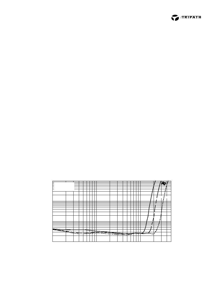
Typical Performance
0.01
10
0.02
0.05
0.1
0.2
0.5
1
2
5
1
500
2
5
10
20
50
100
200
54V
Output Power (W)
THD+N (%)
39V
45V
THD+N versus Output Power versus Supply Voltage
R
L
= 4
f = 1kHz
BBM = 80nS
BW = 22Hz - 22kHz

T E C H N I C A L I N F O R M A T I O N
2
TA3020, Rev 2.1, 01.01
Absolute Maximum Ratings
(Note 1)
SYMBOL PARAMETER
Value
UNITS
VPP, VNN
Supply Voltage
+/- 70
V
V5
Positive 5 V Bias Supply
Voltage at Input Pins (pins 12-16, 18, 19-26, 29-33, 37)
6
-0.3V to (V5+0.3V)
V
VN10
Voltage for FET drive
VNN+13
V
T
STORE
Storage Temperature Range
-55∫ to 150∫
C
T
A
Operating Free-air Temperature Range (Note 2)
-40∫ to 85∫
C
T
J
Junction
Temperature
150∫
C
ESD
HB
ESD Susceptibility ≠ Human Body Model (Note 3)
All pins
TBD
V
ESD
MM
ESD Susceptibility ≠ Machine Model (Note 4)
All pins
TBD
V
Note 1: Absolute Maximum Ratings indicate limits beyond which damage to the device may occur.
See the table below for Operating Conditions.
Note 2: This is a target specification. Characterization is still needed to validate this temperature range.
Note 3: Human body model, 100pF discharged through a 1.5K
resistor.
Note 4: Machine model, 220pF ≠ 240pF discharged through all pins.
Operating Conditions
(Note 5)
SYMBOL PARAMETER MIN.
TYP.
MAX.
UNITS
VPP, VNN
Supply Voltage
+/- 15
+/-45
+/- 65
V
V5
Positive 5 V Bias Supply
4.5
5
5.5
V
VN10
Voltage for FET drive (Volts above VNN)
9
10
12
V
Note 5: Recommended Operating Conditions indicate conditions for which the device is functional.
See Electrical Characteristics for guaranteed specific performance limits.

T E C H N I C A L I N F O R M A T I O N
TA3020, Rev 2.1, 01.01
3
Electrical Characteristics
(Note 6)
T
A
= 25
∞
C. See Application/Test Circuit on page 7. Unless otherwise noted, the supply voltage is
VPP=|VNN|=45V.
SYMBOL PARAMETER
CONDITIONS MIN.
TYP.
MAX.
UNITS
I
q
Quiescent Current
(No load, BBM0=1,BBM1=0,
Mute = 0V)
VPP = +45V
VNN = -45V
V5 = 5V
VN10 = 10V
90
90
45
200
TBD
TBD
mA
mA
mA
mA
I
MUTE
Mute Supply Current
(No load, Mute = 5V)
VPP = +45V
VNN = -45V
V5 = 5V
VN10 = 10V
1
1
20
1
TBD
mA
mA
mA
mA
V
IH
High-level input voltage (MUTE)
3.5
V
V
IL
Low-level input voltage (MUTE)
1.0
V
V
OH
High-level output voltage (HMUTE) I
OH
= 3mA
4.0
V
V
OL
Low-level output voltage (HMUTE) I
OL
= 3mA
0.5
V
V
OFFSET
Output Offset Voltage
No Load, MUTE = Logic low
0.1% R
FBA
, R
FBB
, R
FBC
resistors
-TBD TBD mV
I
OC
Over Current Sense Voltage
Threshold
TBD TBD
1.0
TBD
V
I
VPPSENSE
VPPSENSE Threshold Currents
Over-voltage turn on (muted)
Over-voltage turn off (mute off)
Under-voltage turn off (mute off)
Under-voltage turn on (muted)
TBD
TBD
162
154
79
72
TBD
TBD
µ
A
µ
A
µ
A
µ
A
V
VPPSENSE
Threshold Voltages with
R
VPPSENSE
= XXK
Over-voltage turn on (muted)
Over-voltage turn off (mute off)
Under-voltage turn off (mute off)
Under-voltage turn on (muted)
TBD
TBD
TBD
TBD
TBD
TBD
TBD
TBD
V
V
V
V
I
VNNSENSE
VNNSENSE Threshold Currents
Over-voltage turn on (muted)
Over-voltage turn off (mute off)
Under-voltage turn off (mute off)
Under-voltage turn on (muted)
TBD
TBD
174
169
86
77
TBD
TBD
µ
A
µ
A
µ
A
µ
A
V
VNNSENSE
Threshold Voltages with
R
VNNSENSE
= XXK
Over-voltage turn on (muted)
Over-voltage turn off (mute off)
Under-voltage turn off (mute off)
Under-voltage turn on (muted)
TBD
TBD
TBD
TBD
TBD
TBD
TBD
TBD
V
V
V
V
Note 6:
Minimum and maximum limits are guaranteed but may not be 100% tested.

T E C H N I C A L I N F O R M A T I O N
4
TA3020, Rev 2.1, 01.01
Performance Characteristics ≠ Single Ended
T
A
= 25
∞
C. Unless otherwise noted, the supply voltage is VPP=|VNN|=45V, the input frequency is
1kHz and the measurement bandwidth is 20kHz. See Application/Test Circuit.
SYMBOL PARAMETER
CONDITIONS MIN.
TYP.
MAX.
UNITS
P
OUT
Output
Power
(continuous RMS/Channel)
THD+N = 0.1%, R
L
= 8
R
L
= 4
THD+N = 1%, R
L
= 8
R
L
= 4
100
190
120
220
W
W
W
W
THD + N Total Harmonic Distortion Plus
Noise
P
OUT
= 50W/Channel, R
L
= 8
0.02 %
IHF-IM
IHF Intermodulation Distortion
19kHz, 20kHz, 1:1 (IHF), R
L
= 8
P
OUT
= 30W/Channel
0.03 %
SNR Signal-to-Noise
Ratio
A Weighted, R
L
= 4
,
P
OUT
= 275W/Channel
102 dB
CS Channel
Separation
0dBr = 30W, R
L
= 8
, f = 1kHz
97 dB
Power Efficiency
P
OUT
= 150W/Channel, R
L
= 8
95 %
A
V
Amplifier
Gain
P
OUT
= 10W/Channel, R
L
= 4
See Application / Test Circuit
TBD V/V
A
VERROR
Channel to Channel Gain Error
P
OUT
= 10W/Channel, R
L
= 4
See Application / Test Circuit
0.5
dB
e
NOUT
Output Noise Voltage
A Weighted, no signal, input shorted,
DC offset nulled to zero
260
µ
V
T E C H N I C A L I N F O R M A T I O N
TA3020, Rev 2.1, 01.01
5
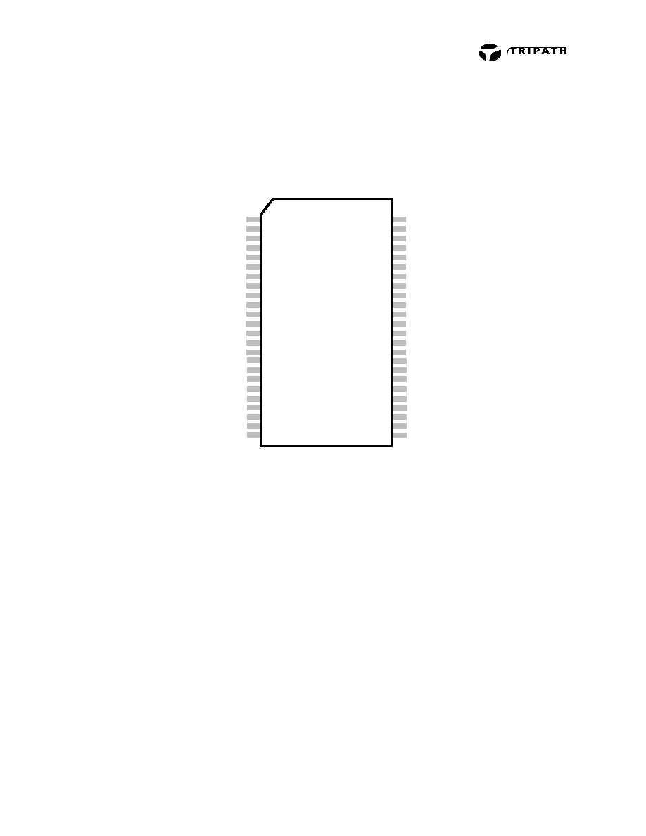
TA3020 Pinout
OCR2
REF1
OCR1
V5
OCR1
VNN
VBOOT1
OCS1LP
OCS1HN
HO1
HO1COM
LO1COM
LO1
LO2
DCOMP
FBKOUT2
HMUTE
FBKGND1
OCR2
NC
VBOOT2
OCS2HN
OCS2HP
OCS2LP
OCS2LN
HO2
HO2COM
LO2COM
42
31
32
33
34
35
36
37
38
39
40
41
1
15
14
13
11
10
12
9
8
7
6
5
4
3
2
48-pin Dip
(Top View)
16
17
18
VN10
48
43
44
45
46
47
OCS1HP
OCS1LN
NC
NC
AGND
FBKOUT1
FBKGND2
BBM1
BBM0
OAOUT2
INV2
21
20
19
22
23
24
BIASCAP
MUTE
INV1
OAOUT1
V5
VPPSENSE
25
26
27
28
29
30
VNNSENSE
AGND