 | –≠–ª–µ–∫—Ç—Ä–æ–Ω–Ω—ã–π –∫–æ–º–ø–æ–Ω–µ–Ω—Ç: TA3021-60 | –°–∫–∞—á–∞—Ç—å:  PDF PDF  ZIP ZIP |

T E C H N I C A L I N F O R M A T I O N
1
Stereo 250W (4
) Class-T Digital Audio Amplifier Driver
using Digital Power Processing
TM
TA3021-60
ADVANCED INFORMATION ≠ July 16, 1999
General Description
The TA3021-60 is a 250W (4
), two-channel Amplifier Driver IC which uses Tripath's
proprietary Digital Power Processing
TM
technology. The TA3021-60 has four
breakthrough features not found in linear amplifier solutions: 1) ability to control and
monitor the amplifier by a two-wire digital serial bus that is compatible with Philips'
I
2
C
TM
bus, 2) a volume control which dramatically reduces total system noise, 3)
optional differential inputs and 4) a mute on silence feature which automatically
mutes the amplifier when no input signal is present. Class-T amplifiers offer both the
audio fidelity of Class-AB and the power efficiency of Class-D amplifiers.
Applications
ÿ
Audio/Video Amplifiers &
Receivers
ÿ
Pro-audio Amplifiers
ÿ
Automobile Power
Amplifiers
ÿ
Subwoofer Amplifiers
Benefits
ÿ
Reduced system cost with
smaller/less expensive
power supply and heat sink
ÿ
Signal fidelity equal to high
quality Class-AB amplifiers
ÿ
High dynamic range
compatible with digital
media such as CD and DVD
ÿ
Integrated volume control
simplifies system design
and reduces output noise
ÿ
Optional control/status
through industry-standard
digital serial bus simplifies
system design
Features
ÿ
Class-T architecture
ÿ
Proprietary Digital Power Processing
technology
ÿ
"Audiophile" Sound Quality
ÿ
0.01% THD+N @ 50W, 8
ÿ
0.02% IHF-IM @ 50W, 8
ÿ
High Efficiency
ÿ
90% @ 125W @ 8
ÿ
85% @ 250W @ 4
ÿ
Supports wide range of output power
levels
ÿ
Up to 250W/channel (4
), single-
ended outputs
ÿ
Up to 1000W (4
), bridged outputs
ÿ
Two modes of control/status operation:
ÿ
1. Through analog pins
ÿ
2. Through digital serial bus
ÿ
Differential or single-ended audio inputs
ÿ
Volume control with 120 dB range in 0.5
dB steps
ÿ
Mute on silence function: mute on
command or after a programmable time
of no input
ÿ
Low output noise: <150
µ
V
ÿ
Simplified power supply design
ÿ
Output over-current protection (Will limit
current before hard shut-down)

T E C H N I C A L I N F O R M A T I O N
2
ÿ
Over- and under-voltage
protection
ÿ
48-pin DIP (dual-inline package)
ÿ
Supports 100kHz frequency response of
Super Audio CD (SACD) and DVD-Audio
T E C H N I C A L I N F O R M A T I O N
3
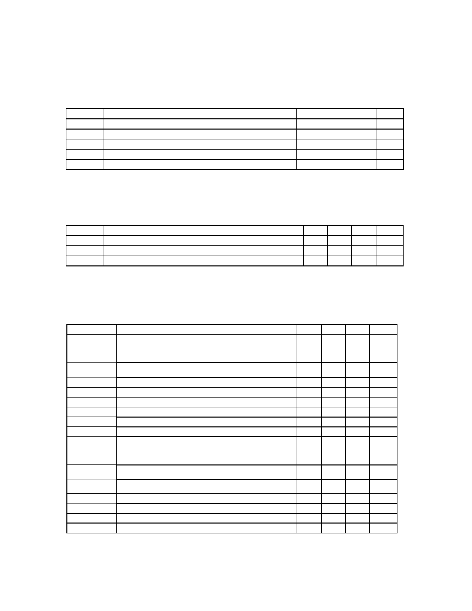
Absolute Maximum Ratings
SYMBOL
PARAMETER
Value
UNITS
Vs
Supply Voltage (Vspos & Vsneg)
+/- 75
V
V5
Positive 5 V Bias Supply
6
V
VN10
Reference Voltage: Nominal +10V referenced to Vsneg
18
V
T
STORE
Storage Temperature Range
-40 to 150
∫C
T
A
Operating Free-air Temperature Range
-20 to +80
∫C
Notes: Absolute Maximum Ratings indicate limits beyond which damage to the device may occur.
Damage will occur to the device if VN10 is not supplied or falls below the recommended
operating voltage when V
S
is within its recommended operating range.
Operating Conditions
SYMBOL
PARAMETER
MIN.
TYP.
MAX.
UNITS
Vs
Supply Voltage (Vspos & Vsneg)
+/- 35
+/- 54
+/- 60
V
V5
Positive 5 V Bias Supply
4.5
5
5.5
V
VN10
Reference Voltage: Nominal +10V referenced to Vsneg
9
10
11
V
Note: Recommended Operating Conditions indicate conditions for which the device is functional. See
Electrical Characteristics for guaranteed specific performance limits.
Electrical Characteristics
T
A
= 25
∞
C. See Notes 1 & 2 for Operating Conditions and Test/Application
Circuit Setup.
SYMBOL
PARAMETER
MIN.
TYP.
MAX.
UNITS
I
q
Quiescent Current
+54V
(no load, BBM0=__, BBM1=__,
-54V
BBM2=__)
+5V
VN10
mA
mA
mA
mA
I
S
Source Current @ P
OUT
= 250W, R
L
= 4
V
SPOS
= +54V
@ 10% THD+N
V
SNEG
= -54V
A
A
I5
Source Current for 5V Bias Supply @ P
OUT
= 250W, R
L
= 4
mA
IVN10
Source Current for VN10 Supply @ P
OUT
= 250W, R
L
= 4
mA
Vu
Under Voltage (Vspos & Vsneg)
+/- 35
V
Vo
Over Voltage (Vspos & Vsneg)
+/- 60
V
V
IH
High-level Input Voltage (MUTE & SLEEP)
3.5
V
V
IL
Low-level Input Voltage (MUTE & SLEEP)
1
V
I
DD
MUTE
Mute Supply Current
+54V
(no load, BBM0=__, BBM1=__,
-54V
BBM2=__)
+5V
VN10
mA
mA
mA
mA
V
OH
High-level Output Voltage (HMUTE/SDA, OVERLOAD/SCL &
PSMUTE)
3.5
V
V
OL
Low-level Output Voltage (HMUTE/SDA, OVERLOAD/SCL &
PSMUTE)
1
V
V
OC-LIMIT
Over Current Sense Voltage Threshold For Current Limiting
0.7
V
V
OC-SD
Over Current Sense Voltage Threshold For Shut-down
1.2
V
A
V
Gain Ratio V
OUT
/V
IN
, R
IN
= 0
V/V
Voffset
Offset Voltage, no load, MUTE = Logic low
10
mV

T E C H N I C A L I N F O R M A T I O N
4
Minimum and maximum limits are guaranteed but may not be 100% tested.

T E C H N I C A L I N F O R M A T I O N
5
Performance Characteristics ≠ Single Ended
Unless otherwise specified, f = 1kHz, Measurement Bandwidth = 22kHz. T
A
=
25
∞
C.
See Notes 1 & 2 for Operating Conditions and Test/Application Circuit Setup.
Minimum and maximum limits are guaranteed but may not be 100% tested.
Notes:
1) V
SPOS
= +54V, V
SNEG
= -54V, V5 = +5V, VN10 = +10V referenced to V
SNEG
2) Test/Application Circuit Values: D = MUR120T3 diodes, R
IN
= ____K
R
D
= 33
, R
S
= 0.025
,
R
G
= 10
L
F
= 18uH (Amidon core T200-2)
C
F
= 0.22uF, C
D
= 0.1uF, C
IN
= 1uF, C
BY
= 0.1uF
Power Output MOSFETs = ST STW38NB20
BBMO=__, BBM1=__, BBM2=___
SYMBOL
PARAMETER
CONDITIONS
MIN.
TYP.
MAX.
UNITS
P
OUT
Output Power
(continuous RMS/Channel)
THD+N = 0.1%, R
L
= 8
R
L
= 4
THD+N = 1%,
R
L
= 8
R
L
= 4
120
250
160
300
W
W
W
W
THD + N
Total Harmonic Distortion Plus
Noise
P
OUT
= 50W/Channel, R
L
= 8
0.01
%
IHF-IM
IHF Intermodulation Distortion
19kHz, 20kHz, 1:1 (IHF), R
L
= 8
P
OUT
= 50W/Channel
0.02
%
SNR
Signal-to-Noise Ratio
A Weighted, R
L
= 4
,
P
OUT
= 250W/Channel
110
dB
CS
Channel Separation
0dBr = 100W, R
L
= 4
, f = 1kHz
80
dB
PSRR
Power Supply Rejection Ratio
Input Referenced, 30kHz Bandwidth
65
dB
Power Efficiency
P
OUT
= 150W/Channel, R
L
= 8
90
%
e
NOUT
Output Noise Voltage
A Weighted, no signal, input shorted,
DC offset nulled to zero
150
µ
V