 | –≠–ª–µ–∫—Ç—Ä–æ–Ω–Ω—ã–π –∫–æ–º–ø–æ–Ω–µ–Ω—Ç: TAA2008 | –°–∫–∞—á–∞—Ç—å:  PDF PDF  ZIP ZIP |

T r i p a t h T e c h n o l o g y, I n c . - T e c h n i c a l I n f o r m a t i o n
1
TAA2008 ≠KLi/1.0/05.06
TAA2008
STEREO 9W (8
) CLASS-TTM DIGITAL AUDIO AMPLIFIER USING
DIGITAL POWER PROCESSINGTM TECHNOLOGY
T E C H N I C A L I N F O R M A T I O N R e v i s i o n 1 . 0 ≠ M a y 2 0 0 6
G E N E R A L D E S C R I P T I O N
The TAA2008 is a 9W/ch continuous average two-channel Class-T Digital Audio Power Amplifier IC
using Tripath's proprietary Digital Power ProcessingTM technology. The TAA2008, in a QFN package,
along with extremely high efficiency, allows for a very compact amplifier design. Class-T amplifiers
offer both the audio fidelity of Class-AB and the power efficiency of Class-D amplifiers.
A P P L I C A T I O N S
LCD TV's
LCD Monitors
Plasma TV's
Computer/PC Multimedia
Battery Powered Systems
B E N E F I T S
Fully integrated solution with FETs
Compact packaging and board design
Reduced system cost with no heat sink
Dramatically improves efficiency versus Class-
AB
Signal fidelity equal to high quality linear
amplifiers
High dynamic range compatible with digital
media such as CD, DVD, and Internet audio
Capable of driving a wide range of load
impedances
T Y P I C A L P E R F O R M A N C E
F E A T U R E S
Class-T architecture
Single Supply Operation
"Audiophile" Quality Sound
0.025% THD+N @ 5W, 8
0.1% IHF-IM @ 1W, 8
6.3W @ 8
, 0.1% THD+N
3.5W @ 16
, 0.1% THD+N
High Power
14.25W @ 6
, 10% THD+N
9W @ 8
, 10% THD+N
5W @ 16
, 10% THD+N
Extremely High Efficiency
89% @ 5W, 16
86% @ 9W, 8
Dynamic Range = 98.5 dB
Mute and Sleep modes
Improved turn-on & turn-off pop
suppression
Over-current protection with automatic
restart circuit
Over-temperature protection
Space saving 32-pin 8mm x 8mm x 1mm
QFN package with exposed pad
0.01
10
0.02
0.05
0.1
0.2
0.5
1
2
5
1
20
2
3
4
5
6
7
8
9 10
VDD = 12V
f = 1kHz
A
V
= 12V/V
BW = 22Hz - 20kHz(AES17)
R
L
=16
R
L
=8
R
L
=6
R
L
=4
THD+N versus Output Power
Output Power (W)
T
HD+
N (
%
)
PGND1
5VGEN
DCAP2
DCAP1
V5D
AGND1
INV2
DGND
PGND2
FAULT
SLEEP
AGND3
BIASCAP
18
17
1
8
7
6
5
4
3
2
OAOUT2
24
19
20
21
22
23
CPUMP
VDDA
9 10 11 12 13 14 15 16
N
C OU
T
P
2
OU
T
M
2
V
DD1
N
C
OU
T
P
1
OU
T
M
1
V
DD2
N
C
MU
TE
IN
V
1
V5
A
AGN
D
2
O
V
RL
DB
RE
F
31
30 29
27 26
28
25
32
OAOU
T
1

T r i p a t h T e c h n o l o g y, I n c . - T e c h n i c a l I n f o r m a t i o n
2
TAA2008 ≠KLi/1.0/05.06
A B S O L U T E M A X I M U M R A T I N G S
(Note 1)
SYMBOL PARAMETER
Value
UNITS
V
DD
Supply Voltage
16
V
V5
Input Section Supply Voltage
6.0
V
SLEEP
SLEEP Input Voltage
-0.3 to 6.0
V
MUTE
MUTE Input Voltage
-0.3 to V5+0.3
V
T
STORE
Storage Temperature Range
-40
to 150
∞C
T
A
Operating Free-air Temperature Range
0 to 70
∞C
T
J
Junction Temperature
150
∞C
ESD
HB
ESD Susceptibility ≠ Human Body Model (Note 2)
2000
V
ESD
MM
ESD Susceptibility ≠ Machine Model (Note 3)
200
V
Note 1: Absolute Maximum Ratings indicate limits beyond which damage to the device may occur.
Note 2: Human body model, 100pF discharged through a 1.5K
resistor.
Note 3: Machine model, 220pF ≠ 240pF discharged through all pins.
O P E R A T I N G C O N D I T I O N S
(Note 4)
SYMBOL PARAMETER MIN.
TYP.
MAX.
UNITS
V
DD
Supply Voltage (Note 5)
8.5
12
14.0
V
V
IH
High-level Input Voltage (MUTE, SLEEP)
3.5
V
V
IL
Low-level Input Voltage (MUTE, SLEEP)
1
V
Note 4: Recommended Operating Conditions indicate conditions for which the device is functional. See
Electrical Characteristics for guaranteed specific performance limits.
Note 5: Operation above 13.2V requires the use of low and high side schottky diodes as well as 220uF for
C
SW
. See the Application Section for additional information
T H E R M A L C H A R A C T E R I S T I C S
SYMBOL PARAMETER
VALUE UNITS
JA
Junction-to-ambient Thermal Resistance (note 6)
22
∞C/W
Note 6: The
JA
value is based on the exposed pad being soldered down to the printed circuit board. The
exposed pad must be soldered to an exposed copper area on the printed circuit board for proper thermal
and electrical performance.

T r i p a t h T e c h n o l o g y, I n c . - T e c h n i c a l I n f o r m a t i o n
3
TAA2008 ≠KLi/1.0/05.06
E L E C T R I C A L C H A R A C T E R I S T I C S
(Note 7)
See Test/Application Circuit. Unless otherwise specified, V
DD
= 12V, f = 1kHz, Measurement
Bandwidth = 20kHz, R
L
= 8
, T
A
= 25
∞C, package exposed pad soldered to the printed circuit
board.
SYMBOL PARAMETER
CONDITIONS MIN.
TYP.
MAX.
UNITS
P
O
Output Power
(Continuous Average/Channel)
THD+N = 0.1% R
L
= 6
R
L
= 8
R
L
= 16
THD+N = 10% R
L
= 6
R
L
= 8
R
L
= 16
VDD = 13.2V, THD+N=10%
R
L
= 6
R
L
= 8
R
L
= 16
TBD
8
6.3
3.5
12
9
5
14.25
12
6.3
W
W
W
W
W
W
W
W
W
I
DD,MUTE
Mute Supply Current
MUTE = V
IH
31
36
mA
I
DD, SLEEP
Sleep Supply Current
SLEEP = V
IH
0.25
2
mA
I
q
Quiescent Current
V
IN
= 0 V
61
75
mA
THD + N Total Harmonic Distortion Plus
Noise
P
O
= 5W/Channel
0.022
%
IHF-IM
IHF Intermodulation Distortion
19kHz, 20kHz, 1:1 (IHF)
0.1
0.5
%
SNR Signal-to-Noise
Ratio
A-Weighted, P
OUT
= 9W, R
L
= 8
98.5
dB
CS
Channel Separation
f = 1 kHz
20 Hz
<
f
<
20 kHz
50
85
60
dB
dB
PSRR
Power Supply Rejection Ratio
VDD = 9V to 13.2V
Vripple = 100mVrms, f=1kHz
65 75
65
dB
dB
Power Efficiency
P
OUT
= 5W/Channel, R
L
= 16
89 %
V
OFFSET
Output Offset Voltage
No Load, MUTE = Logic Low
50
150
mV
V
OH
High-level output voltage
(FAULT & OVERLOAD)
3.5
V
V
OL
Low-level output voltage
(FAULT & OVERLOAD)
1
V
e
OUT
Output Noise Voltage
A-Weighted, input AC grounded
100
150
µV
Note 7: Minimum and maximum limits are guaranteed but may not be 100% tested.

T r i p a t h T e c h n o l o g y, I n c . - T e c h n i c a l I n f o r m a t i o n
4
TAA2008 ≠KLi/1.0/05.06
P I N D E S C R I P T I O N
T A A 2 0 0 8 P I N O U T
Pin
Function
Description
1, 29
OAOUT2, OAOUT1
Input stage output pins.
2, 30
INV2, INV1
Single-ended inputs. Inputs are a "virtual" ground of an inverting opamp with
approximately 2.4VDC bias.
3
BIASCAP
Input stage bias voltage (approximately 2.4VDC).
4, 24,
27
AGND3, AGND1,
AGND2
Analog Ground
5
SLEEP
When set to logic high, device goes into low power mode. If not used, this pin
should be grounded
6
FAULT
A logic high output indicates thermal overload, or an output is shorted to ground,
or another output.
7, 18
PGND2, PGND1
Power Grounds (high current)
8
DGND
Digital Ground. Connect to AGND locally (near the TAA2008).
10, 12;
15, 13
OUTP2 & OUTM2;
OUTP1 & OUTM1
Bridged output pairs
11, 14
VDD2, VDD1
Supply pins for high current H-bridges, nominally 12VDC.
17
VDDA
Analog 12VDC. Connect to same supply as VDD1 and VDD2.
19
CPUMP
Charge pump output (nominally 10V above VDDA)
20
5VGEN
Regulated 5VDC source used to supply power to the input section (pins 23 and
28).
21,22
DCAP2, DCAP1
Charge pump switching pins. DCAP1 (pin 22) is a free running 300kHz square
wave between VDDA and DGND (12Vpp nominal). DCAP2 (pin 21) is level
shifted 10 volts above DCAP1 (pin 22) with the same amplitude (12Vpp nominal),
frequency, and phase as DCAP1.
23, 28
V5D, V5A
Digital 5VDC, Analog 5VDC
25
REF
Internal reference voltage; approximately 1.0 VDC.
26
OVERLOADB
A logic low output indicates the input signal has overloaded the amplifier.
31
MUTE
When set to logic high, both amplifiers are muted and in idle mode. When low
(grounded), both amplifiers are fully operational. If left floating, the device stays in
the mute mode. This pin should be tied to GND if not used.
9, 16, 32
NC
Not connected. Not bonded internally.
PGND1
5VGEN
DCAP2
DCAP1
V5D
AGND1
INV2
DGND
PGND2
FAULT
SLEEP
AGND3
BIASCAP
18
17
1
8
7
6
5
4
3
2
32-pin QFN
(Top View)
OAOUT2
24
19
20
21
22
23
CPUMP
VDDA
9
10
11
12
13
14
15
16
NC
OUT
P
2
OUT
M
2
V
DD1
NC
OUT
P
1
OUT
M
1
V
DD2
NC
MUT
E
IN
V1
V5A
AG
N
D
2
OV
RL
DB
RE
F
31
30
29
27
26
28
25
32
OA
OUT
1

T r i p a t h T e c h n o l o g y, I n c . - T e c h n i c a l I n f o r m a t i o n
5
TAA2008 ≠KLi/1.0/05.06
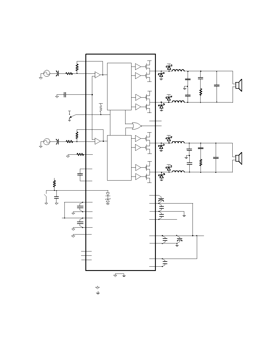
A P P L I C A T I O N / T E S T C I R C U I T
T AA2008
R
L
8
or 16
MUTE
FA ULT (c onnect to MUTE f or auto restart)
OV ERLOA DB
(+12V )
C
I
2.2uF
OA OUT1
OA OUT2
INV 1
INV 2
OUTP1
OUTM1
OUTP2
OUTM2
V DDA
5V GEN
BIA SCA P
DCA P2
DCA P1
C
I
2.2uF
C
A
0.1uF
C
D
0.1uF
CPUMP
29
30
7
20
17
14
11
26
6
15
13
10
12
19
21
22
2
1
31
3
R
F
20K
5
R
Z
10
,
1/4W
R
Z
10
,
1/4W
C
Z
0.22uF
C
P
1uF
+
+
5V
SLEEP
5V
5V
+12V
0.1uF
REF
R
RE F
8.25K
, 1%
25
1M
** For V DD v oltages abov e 13.2V , output diodes (D
O
) should be used
and the value of C
S W
should be inc reas ed to 220uF. A ll Diodes are
Motorola MBRS130T3 or equivalent.
V DD1
PGND1
V DD1
PGND1
V DD2
V DD2
PGND2
PGND2
Note: A nalog and Digital/Pow er Grounds must
be connected loc ally at the TA A 2008
C
S
0.1uF
C
S
0.1uF
To Pin 20
23
24
V 5D
27
A GND1
A GND2
V5A
8
C
S
0.1uF
DGND
V DD1
PGND2
18
PGND1
V DD2
V DD
+
+
Proces s ing
&
Modulation
Proces s ing
&
Modulation
C
o
0.22uF
L
o
10uH, 2A
28
(Pin 4)
A nalog Ground
Digital/Pow er Ground
(Pin 18)
(Pin 18)
(Pin 7)
(Pin 7)
To Pins 23,28
R
I
20K
(Pin 24)
R
F
20K
R
I
20K
A GND3
4
100uF, 16V
C
S W
**
C
o
0.22uF
L
o
10uH, 2A
R
L
8
or 16
L
o
10uH, 2A
L
o
10uH, 2A
C
o
0.22uF
C
o
0.22uF
C
Z
0.22uF
C
SW
0.1uF
C
SW
0.1uF
C
S
0.1uF
D
O
**
D
O
**
C
DO
0.01uF
(Pin 18)
(Pin 7)
9
NC
16
32
C
DO
0.01uF
NC
NC
D
O
**
D
O
**
V DD1
V DD2
V DD2
V DD1
N.C.
