 | –≠–ª–µ–∫—Ç—Ä–æ–Ω–Ω—ã–π –∫–æ–º–ø–æ–Ω–µ–Ω—Ç: TAA2009 | –°–∫–∞—á–∞—Ç—å:  PDF PDF  ZIP ZIP |
Tripath Technology, Inc. - Technical Information
1
TAA2009 ≠KLi/1.02/ 05.06
TAA2009
STEREO 9W (8
) CLASS-TTM DIGITAL AUDIO AMPLIFIER USING
DIGITAL POWER PROCESSINGTM TECHNOLOGY
T E C H N I C A L I N F O R M A T I O N R e v i s i o n 1 . 0 2 ≠ M a y 2 0 0 6
G E N E R A L D E S C R I P T I O N
The TAA2009 is a 9W/ch continuous average two-channel Class-T Digital Audio Power Amplifier IC
using Tripath's proprietary Digital Power ProcessingTM technology. The TAA2009, in a QFN package,
along with extremely high efficiency, allows for a very compact amplifier design. Class-T amplifiers
offer both the audio fidelity of Class-AB and the power efficiency of Class-D amplifiers.
A P P L I C A T I O N S
LCD TV's
LCD Monitors
Plasma TV's
Computer/PC Multimedia
Battery Powered Systems
B E N E F I T S
Fully integrated solution with FETs
Compact packaging and board design
Reduced system cost with no heat sink
Differential inputs minimize common-mode
noise
Dramatically improves efficiency versus Class-
AB
Signal fidelity equal to high quality linear
amplifiers
High dynamic range compatible with digital
media such as CD, DVD, and Internet audio
Capable of driving a wide range of load
impedances
Sophisticated pop reduction circuit
T Y P I C A L P E R F O R M A N C E
F E A T U R E S
Class-T architecture
Single Supply Operation
"Audiophile" Quality Sound
0.05% THD+N @ 5W, 8
0.16% IHF-IM @ 1W, 8
6.4W @ 8
, 0.1% THD+N
3.5W @ 16
, 0.1% THD+N
High Power
10.6W @ 6
, 10% THD+N
9W @ 8
, 10% THD+N
5W @ 16
, 10% THD+N
Extremely High Efficiency
90% @ 5W, 16
86% @ 9W, 8
Dynamic Range = 96 dB
Mute and Sleep modes
Improved turn-on & turn-off pop
suppression
Over-current protection with automatic
restart circuit
Over-temperature protection
Space saving 32-pin 8mm x 8mm x 1mm
QFN package with exposed pad
Filterless Operation Option
1
9
2
3
4
5
6
7 8
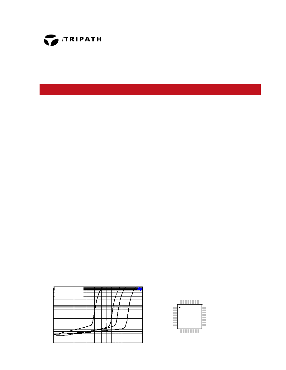
THD+N versus Output Power
TH
D
+
N
(
%
)
Output Power (W)
VDD = 12V
f = 1kHz
Gain1=0, Gain0=1
BW = 22Hz - 20kHz(AES17)
10
5
1
2
0.1
0.2
0.5
0.05
0.02
0.01
10
20
R
L
= 16
R
L
= 8
R
L
= 6
R
L
= 4
CPUMP
VDDA
5VGEN
GAIN1
AGND
IN2P
V5D
FAULT
MUTE
SLEEP
REF
DGND
GAIN0
18
17
1
8
7
6
5
4
3
2
32-pin QFN
(Top View)
IN1P
24
19
20
21
22
23
DCAP
SUB
9
10
11
12
13
14
15
16
OUTP
1
VDD
1
OU
T
M
1
PG
ND
2
OU
T
P
2
VD
D2
OU
T
M
2
PG
N
D
1
IN
1
M
C1
AG
ND
V5
A
IN
L
C2
IN
2
M
31
30
29
27
26
28
25
32
BIASCAP
Tripath Technology, Inc. - Technical Information
2
TAA2009 ≠KLi/1.02/ 05.06
A B S O L U T E M A X I M U M R A T I N G S
(Note 1)
SYMBOL PARAMETER
Value
UNITS
V
DD
Supply Voltage (note 1)
14
V
MUTE, SLEEP,
GAIN1, GAIN0, INL
MUTE Input Voltage
-0.3 to V5 + 0.3
V
T
STORE
Storage Temperature Range
-40
to 150
∞C
T
A
Operating Free-air Temperature Range
-40 to +85
∞C
ESD
HB
ESD Susceptibility ≠ Human Body Model (Note 2)
1500
V
Note 1: Absolute Maximum Ratings indicate limits beyond which damage to the device may occur. Please
note that this is not a valid "operating condition". The maximum voltage on the VDD pins during operation
is 13.2V. Refer to the Maximum Supply Voltage section on page 13.
Note 2: Human body model, 100pF discharged through a 1.5K
resistor.
O P E R A T I N G C O N D I T I O N S
(Note 3)
-40
o
C to +85
O
C
SYMBOL PARAMETER MIN.
TYP.
MAX.
UNITS
V
DD
Supply Voltage (note 1)
8.5
12
13.2
V
V
IH
High-level Input Voltage (MUTE, SLEEP, GAIN1, GAIN0, INL)
4.2
V
V
IL
Low-level Input Voltage (MUTE, SLEEP, GAIN1, GAIN0, INL)
1.0
V
Note 3: Recommended Operating Conditions indicate conditions for which the device is functional. See
Electrical Characteristics for guaranteed specific performance limits.
T H E R M A L C H A R A C T E R I S T I C S
SYMBOL PARAMETER
VALUE UNITS
JA
Junction-to-ambient Thermal Resistance (note 4)
21
∞C/W
Note 4: The
JA
value is based on the exposed pad being soldered down to the printed circuit board. The
exposed pad must be soldered to an exposed copper area on the printed circuit board for proper thermal
and electrical performance. The exposed pad is at substrate ground.
Tripath Technology, Inc. - Technical Information
3
TAA2009 ≠KLi/1.02/ 05.06
E L E C T R I C A L C H A R A C T E R I S T I C S
(Note 5)
See Application/Test Circuit with single ended inputs and filtered outputs. Unless otherwise specified,
V
DD
= 12V, f = 1kHz, Gain1=0, Gain0=1 Measurement Bandwidth = 20kHz, R
L
= 8
, T
A
= 25
∞C,
package exposed pad soldered to the printed circuit board.
SYMBOL PARAMETER
CONDITIONS
MIN.
TYP.
MAX.
UNITS
P
O
Output Power
(Continuous
Average/Channel)
THD+N = 0.1% R
L
= 6
R
L
= 8
R
L
= 16
THD+N = 10% R
L
= 6
R
L
= 8
R
L
= 16
7.8
6.4
3.5
10.6
9
5
W
W
W
W
W
W
I
DD,MUTE
Mute Supply Current
MUTE = V
IH
28
mA
I
DD, SLEEP
Sleep Supply Current
SLEEP = V
IH
7
mA
I
q
Quiescent Current
V
IN
= 0 V
60
mA
THD + N Total Harmonic Distortion
Plus Noise
P
O
= 5W/Channel
0.05
%
IHF-IM IHF
Intermodulation
Distortion
19kHz, 20kHz, 1:1 (IHF), Po = 1W
0.16
%
SNR Signal-to-Noise
Ratio A-Weighted, P
OUT
= 9W, R
L
= 8
96
dB
CS
Channel Separation
f = 1 kHz
20 Hz
<
f
<
20 kHz
96
70
dB
dB
PSRR
Power Supply Rejection
Ratio
VDD = 9V to 13.2V
85
dB
Power Efficiency
P
OUT
= 9W/Channel, R
L
= 8
86 %
V
OFFSET1
Dynamic Output Offset
Voltage (note 6)
MUTE transition from high to low
-10
10
mV
V
OFFSET2
Static Output Offset Voltage MUTE = low
50
mV
V
OH
High-level output voltage
(FAULT)
-40
∞C to +85∞C, I
OH
= 250uA
4.5 V
V
OL
Low-level output voltage
(FAULT)
-40
∞C to +85∞C, I
OL
= 250uA
0.5
V
e
OUT
Output Noise Voltage
A-Weighted, input AC grounded
160
µV
Note 5: Minimum and maximum limits are guaranteed but may not be 100% tested.
Note 6: Refer to the Dynamic DC Offset Calibration section on page 14 for a detailed description of
Dynamic Offset Voltage.

Tripath Technology, Inc. - Technical Information
4
TAA2009 ≠KLi/1.02/ 05.06
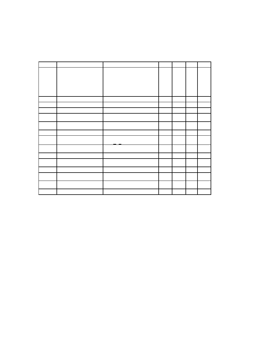
T A A 2 0 0 9 P I N O U T
CPUMP
VDDA
5VGEN
GAIN1
AGND
IN2P
V5D
FAULT
MUTE
SLEEP
REF
DGND
GAIN0
18
17
1
8
7
6
5
4
3
2
32-pin QFN
(Top View)
IN1P
24
19
20
21
22
23
DCAP
SUB
9
10
11
12
13
14
15
16
OUT
P
1
V
DD1
OU
T
M
1
P
G
ND2
OU
T
P
2
V
DD2
OU
T
M
2
P
G
ND1
IN1M
C1
AGND
V5A
INL
C2
IN2M
31
30
29
27
26
28
25
32
BI
A
S
C
A
P

Tripath Technology, Inc. - Technical Information
5
TAA2009 ≠KLi/1.02/ 05.06
P I N D E S C R I P T I O N
Pin
Function
Description
1, 24
IN1P, IN2P
Positive audio input for channel 1 and channel 2
2, 28
V5D, V5A
Digital 5VDC, Analog 5VDC
3, 22
GAIN0, GAIN1
Gain select bits. GAIN0 is least significant bit. See Applications Information for
programmable gain values. Both GAIN 0 and GAIN1 have internal 50K
pull-
down resistors.
4
DGND
Digital Ground. Connect to AGND locally (near the TAA2009).
5
REF
Internal reference voltage; approximately 1.0 VDC.
6
SLEEP
When set to logic high, device goes into low power mode. If not used, this pin
should be grounded
7
MUTE
When set to logic high, both amplifiers are muted and in idle mode. When low
(grounded), both amplifiers are fully operational. If left floating, the device stays in
the mute mode. This pin should be tied to GND if not used.
8
FAULT
A logic high output indicates an under-voltage condition, thermal overload, and an
output is shorted to ground, or another output.
9, 12
16, 13
OUTP1 & OUTM1
OUTP2 & OUTM2
Bridged output pairs
10, 15
VDD1, VDD2
Supply pins for high current H-bridges, nominally 12VDC.
11, 14
PGND1, PGND2
Power Grounds (high current)
17
SUB
Substrate connection. Connect to PGND.
18
CPUMP
Charge pump input (nominally 10V above VDDA)
19
DCAP
Charge pump switching output pin. DCAP is a free running 350kHz square wave
between VDDA and DGND (12Vpp nominal).
20
VDDA
Power supply for analog VDD circuitry. Connect to same supply as VDD1 and
VDD2.
21
5VGEN
Regulated 5VDC source used to supply power to the input section (pins 2 and 28).
23, 30
AGND, AGND
Analog Ground. Connect all pins together directly at the TAA2009.
25, 32
IN2M, IN1M
Negative audio input for channel 2 and channel 1.
26, 31
C2, C1
Pop minimization capacitor. Use 10uF.
27
INL
Modulation selection pin. Connecting the INL pin to a logic high level enables the
inductor-less mode. This mode allows the TAA2009 to be operated without an
output filter as the switching outputs are in phase with zero input. If INL is tied to
a logic low or left floating (pulled down via internal 50K
resistor to ground), the
INL mode will be disabled. This results in a differential output switching pattern
typical of previous Tripath generation parts such as TA2024 and TAA2008. The
state of the INL pin should only be changed with MUTE at a logic high state.
29
BIASCAP
Input stage bias voltage (approximately 2.4VDC).