 | –≠–ª–µ–∫—Ç—Ä–æ–Ω–Ω—ã–π –∫–æ–º–ø–æ–Ω–µ–Ω—Ç: TC2001 | –°–∫–∞—á–∞—Ç—å:  PDF PDF  ZIP ZIP |
T r i p a t h T e c h n o l o g y, I n c . - T e c h n i c a l I n f o r m a t i o n
1
TK2150 ≠ Rev. 1.0/12.02
TK2150
STEREO 200W (6
) CLASS-T DIGITAL AUDIO AMPLIFIER DRIVER
USING DIGITAL POWER PROCESSING
T M
TECHNOLOGY
T e c h n i c a l I n f o r m a t i o n - P r e l i m i n a r y R e v i s i o n 1 . 0 ≠ D e c e m b e r 2 0 0 2
G E N E R A L D E S C R I P T I O N
T h e T K 2 1 5 0 ( T C 2 0 0 1 / T P 2 1 5 0 c h i p s e t ) i s a t w o - c h a n n e l , 2 0 0 W ( 6
) p e r c h a n n e l A m p l i f i e r
D r i v e r t h a t u s e s T r i p a t h ' s p r o p r i e t a r y D i g i t a l P o w e r P r o c e s s i n g ( D P P
T M
) t e c h n o l o g y .
C l a s s - T a m p l i f i e r s o f f e r b o t h t h e a u d i o f i d e l i t y o f C l a s s - A B a n d t h e p o w e r e f f i c i e n c y o f
C l a s s - D a m p l i f i e r s .
Applications
Powered DVD Players
Audio/Video Amplifiers & Receivers
Automobile Power Amplifiers
Subwoofer Amplifiers
Pro-audio Amplifiers
Benefits
Reduced system cost with smaller/less
expensive power supply and heat sink
Signal fidelity equal to high quality
Class-AB amplifiers
High dynamic range compatible with
digital media such as CD and DVD
Features
Class-T architecture
Pin compatible with Tripath TK2350 Chipset
Proprietary Digital Power Processing technology
"Audiophile" Sound Quality
0.012% THD+N @ 60W, 8
0.02% IHF-IM @ 30W, 8
High Efficiency
93% @ 120W @ 8
91% @ 150W @ 6
Supports wide range of output power levels
Up to 200W/channel (6
), single-ended outputs,
@+/- 45V
Up to 400W (8
), bridged outputs, @+/- 30V
Output over-current protection
Over- and under-voltage protection
Over-temperature protection
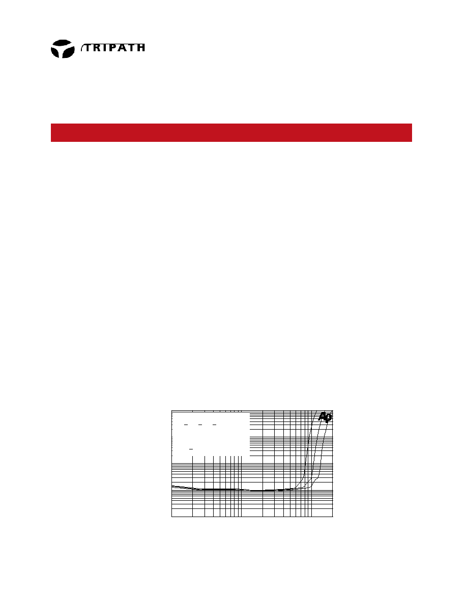
Typical Performance for TK2150
THD+N versus Output Power versus Supply Voltage
0.001
10
0.002
0.005
0.01
0.02
0.05
0.1
0.2
0.5
1
2
5
%
2
200
5
10
20
50
100
W
R
L
= 6
Vs = +35V, +40V, +45V
f = 1kHz
BBM = 40nS
BW = 22hZ - 20kHz(AES17)
NOTE: +45V test uses R
F BC
=11k
(see Application/ Test Circuit)
1
T r i p a t h T e c h n o l o g y, I n c . - T e c h n i c a l I n f o r m a t i o n
2
TK2150 ≠ Rev. 1.0/12.02
Absolute Maximum Ratings TC2001
(Note 1)
SYMBOL PARAMETER
Value
UNITS
V
5
5V Power Supply
6
V
Vlogic
Input Logic Level
V
5
+0.3V V
TA
Operating Free-air Temperature Range
-40∞ to +85∞
∞C
T
STORE
Storage Temperature Range
-55∞ to 150∞
∞C
T
JMAX
Maximum Junction Temperature
150∞
∞C
ESD
HB
ESD Susceptibility ≠ Human Body Model (Note 2)
All pins
2000
V
Note 1: Absolute Maximum Ratings indicate limits beyond which damage to the device may occur.
See the table below for Operating Conditions.
Note 2: Human body model, 100pF discharged through a 1.5K
resistor.
Absolute Maximum Ratings TP2150
(Note 3)
SYMBOL PARAMETER
Value
UNITS
VPP, VNN
Supply Voltage
+/- 65
V
VN10
Voltage for FET drive
VNN+13
V
T
STORE
Storage Temperature Range
-55∫ to 150∫
∞C
T
A
Operating Free-air Temperature Range (Note 4)
-40∫ to 85∫
∞C
T
J
Junction
Temperature
150∫
∞C
ESD
HB
ESD Susceptibility ≠ Human Body Model (Note 5)
All pins
2000
V
ESD
MM
ESD Susceptibility ≠ Machine Model (Note 6)
All pins
TBD
V
Note 3: Absolute Maximum Ratings indicate limits beyond which damage to the device may occur.
See the table below for Operating Conditions.
Note 4: This is a target specification. Characterization is still needed to validate this temperature range.
Note 5: Human body model, 100pF discharged through a 1.5K
resistor.
Note 6: Machine model, 220pF ≠ 240pF discharged through all pins.
Operating Conditions TC2001
(Note 7)
SYMBOL PARAMETER MIN.
TYP.
MAX.
UNITS
V
5
Supply Voltage
4.5
5
5.5
V
V
HI
Logic Input High
V5-1.0
V
V
LO
Logic Input Low
1
V
T
A
Operating Temperature Range
-40
∞ 25∞ 85∞
∞C
Note 7: Recommended Operating Conditions indicate conditions for which the device is functional.
See Electrical Characteristics for guaranteed specific performance limits.
Operating Conditions TP2150
(Note 8)
SYMBOL PARAMETER MIN.
TYP.
MAX.
UNITS
VPP, VNN
Supply Voltage
+/- 15
+/-30
+/- 60
V
VN10
Voltage for FET drive (Volts above VNN)
9
10
12
V
Note 8: Recommended Operating Conditions indicate conditions for which the device is functional.
See Electrical Characteristics for guaranteed specific performance limits.
T r i p a t h T e c h n o l o g y, I n c . - T e c h n i c a l I n f o r m a t i o n
3
TK2150 ≠ Rev. 1.0/12.02
Operating Characteristics TC2001
(Note 9)
SYMBOL PARAMETER MIN.
TYP.
MAX.
UNITS
I5
Supply Current
50
mA
V
IN
Input
Sensitivity
0
1.5
V
V
OUTHI
High Output Voltage
V
5
-0.5
V
V
OUTLO
Low Output Voltage
100
mV
Input DC Bias
2.4
V
Note 9: Recommended Operating Conditions indicate conditions for which the device is functional.
See Electrical Characteristics for guaranteed specific performance limits.
Thermal Characteristics TC2001
SYMBOL PARAMETER
Value
UNITS
JA
Junction-to-ambient Thermal Resistance (still air)
80
∞
C/W
Thermal Characteristics TP2150
SYMBOL PARAMETER
Value
UNITS
JC
Junction-to-case Thermal Resistance
TBD
∞
C/W
Electrical Characteristics TC2001
(Note 10)
T
A
= 25
∞C. See Application/Test Circuit on page 7. Unless otherwise noted, the supply voltage is
VPP=|VNN|=45V.
SYMBOL PARAMETER
CONDITIONS MIN.
TYP.
MAX.
UNITS
I
q
Quiescent Current
(Mute = 0V)
V5 = 5V
45
60
mA
I
MUTE
Mute Supply Current
(Mute = 5V)
V5 = 5V
20
25 mA
V
IH
High-level input voltage (MUTE)
3.5
V
V
IL
Low-level input voltage (MUTE)
1.0
V
V
OH
High-level output voltage (HMUTE) I
OH
= 3mA
4.0
V
V
OL
Low-level output voltage (HMUTE) I
OL
= 3mA
0.5
V
V
TOC
Over Current Sense Voltage
Threshold
TBD TBD
1.0
TBD
V
I
VPPSENSE
VPPSENSE Threshold Currents
Over-voltage turn on (muted)
Over-voltage turn off (mute off)
Under-voltage turn off (mute off)
Under-voltage turn on (muted)
138
62
162
154
79
72
178
87
µA
µA
µA
µA
V
VPPSENSE
Threshold Voltages with
R
VPP1
= R
VPP1
= 357K
(Note 11, Note 12)
Over-voltage turn on (muted)
Over-voltage turn off (mute off)
Under-voltage turn off (mute off)
Under-voltage turn on (muted)
49.3
22.1
57.8
55.0
28.2
25.7
63.5
31.1
V
V
V
V
I
VNNSENSE
VNNSENSE Threshold Currents
Over-voltage turn on (muted)
Over-voltage turn off (mute off)
Under-voltage turn off (mute off)
Under-voltage turn on (muted)
152
65
174
169
86
77
191
95
µA
µA
µA
µA
V
VNNSENSE
Threshold Voltages with
R
VNN1
= 324K
R
VNN2
= 976K
(Note 11, Note 12)
Over-voltage turn on (muted)
Over-voltage turn off (mute off)
Under-voltage turn off (mute off)
Under-voltage turn on (muted)
-49.2
-21.1
-56.4
-54.8
-27.9
-24.9
-61.9
-30.8
V
V
V
V
Note 10: Minimum and maximum limits are guaranteed but may not be 100% tested.

T r i p a t h T e c h n o l o g y, I n c . - T e c h n i c a l I n f o r m a t i o n
4
TK2150 ≠ Rev. 1.0/12.02
Note 11: These supply voltages are calculated using the IVPPSENSE and IVNNSENSE values shown in the
Electrical Characteristics table. The typical voltage values shown are calculated using a RVPP and RVNN
values without any tolerance variation. The minimum and maximum voltage limits shown include either a
+1% or ≠1% (+1% for Over-voltage turn on and Under-voltage turn off, -1% for Over-voltage turn off and
Under-voltage turn on) variation of RVPP or RVNN off the nominal 357kohm, 324kohm, and 976kohm
values. These voltage specifications are examples to show both typical and worst case voltage ranges for
the given RVPP and RVNN resistor values. Please refer to the Application Information section for a more
detailed description of how to calculate the over and under voltage trip voltages for a given resistor value.
Note 12: The fact that the over-voltage turn on specifications exceed the absolute maximum of +/-60V for the TK2150
does not imply that the part will work at these elevated supply voltages. It also does not imply that the
TK2150 is tested or guaranteed at these supply voltages. The supply voltages are simply a calculation
based on the process spread of the IVPPSENSE and IVNNSENSE currents (see note 7). The supply
voltage must be maintained below the absolute maximum of +/-60V or permanent damage to the TK2150
may occur.
Electrical Characteristics TP2150
(Note 13)
T
A
= 25
∞C. See Application/Test Circuit on page 7. Unless otherwise noted, the supply voltage is
VPP=|VNN|=45V.
SYMBOL PARAMETER
CONDITIONS MIN.
TYP.
MAX.
UNITS
I
q
Quiescent Current
(No load, BBM0=1,BBM1=0,
Mute = 0V)
VPP = +45V
VNN = -45V (Note 14)
25
45
mA
mA
I
MUTE
Mute Supply Current
(No load, Mute = 5V)
VPP = +45V
VNN = -45V
1
1
mA
mA
Note 13: Minimum and maximum limits are guaranteed but may not be 100% tested.
Note 14: The difference in the VPP and VNN current draw is due to the VN10 regulator sourcing current to the
VNN supply.
Performance Characteristics TK2150 ≠ Single Ended
T
A
= 25
∞C. Unless otherwise noted, the supply voltage is VPP=|VNN|=45V, the input frequency is 1kHz
and the measurement bandwidth is 20kHz. See Application/Test Circuit.
SYMBOL PARAMETER
CONDITIONS MIN.
TYP.
MAX.
UNITS
P
OUT
Output
Power
(continuous RMS/Channel)
THD+N = 0.1%, R
L
= 8
R
L
= 6
THD+N = 1%,
R
L
= 8
R
L
= 6
100
135
120
155
W
W
W
W
THD + N Total Harmonic Distortion Plus
Noise
P
OUT
= 70W/Channel, R
L
= 8
0.012 %
IHF-IM
IHF Intermodulation Distortion
19kHz, 20kHz, 1:1 (IHF), R
L
= 8
P
OUT
= 30W/Channel
0.02 %
SNR Signal-to-Noise
Ratio
A Weighted, R
L
= 6
,
P
OUT
= 155W/Channel
104.5 dB
CS Channel
Separation
0dBr = 30W, R
L
= 8
, f = 1kHz
92 dB
Power Efficiency
P
OUT
= 150W/Channel, R
L
= 8
93 %
A
V
Amplifier
Gain
P
OUT
= 10W/Channel, R
L
= 6
See Application / Test Circuit
13.3 V/V
A
VERROR
Channel to Channel Gain Error
P
OUT
= 10W/Channel, R
L
= 6
See Application / Test Circuit
0.5
dB
e
NOUT
Output Noise Voltage
A Weighted, no signal, input shorted,
DC offset nulled to zero, R
FBC
= 11k
180
µV
V
OFFSET
Output Offset Voltage
No Load, Mute = Logic Low
0.1% R
FBA
, R
FBB
, R
FBC
resistors
-1.0 1.0 V
T r i p a t h T e c h n o l o g y, I n c . - T e c h n i c a l I n f o r m a t i o n
5
TK2150 ≠ Rev. 1.0/12.02
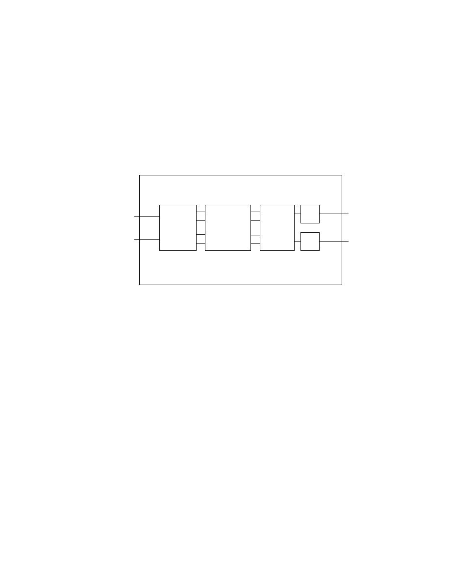
TK2150 Block Diagram
TC2001
Audio
Signal
Processor
TP2150
MOSFET
Driver
Output
MOSFETs
LC
Filter
LC
Filter
Input Left
Input Right
Output Left
Output Right