 | –≠–ª–µ–∫—Ç—Ä–æ–Ω–Ω—ã–π –∫–æ–º–ø–æ–Ω–µ–Ω—Ç: TDA1400 | –°–∫–∞—á–∞—Ç—å:  PDF PDF  ZIP ZIP |

T r i p a t h T e c h n o l o g y, I n c . - P r e l i m i n a r y I n f o r m a t i o n
1
T D A 1 4 0 0 ≠ R e v . 0 . 6 5 / K L i / 0 2 . 0 6
TDA1400
MONO CLASS-T DIGITAL AUDIO AMPLIFIER DRIVER USING
DIGITAL POWER PROCESSING
T M
TECHNOLOGY
P r e l i m i n a r y I n f o r m a t i o n R e v i s i o n 0 . 6 5 ≠ F e b r u a r y 2 0 0 6
G E N E R A L D E S C R I P T I O N
The TDA1400 is a one-channel, Amplifier Driver that uses Tripath's proprietary Digital Power Processing
(DPP
TM
) technology. The TDA1400 offers higher integration over previous Tripath amplifiers driver
chipsets while providing exceptional audio performance for real world applications. Class-T amplifiers
offer both the audio fidelity of Class-AB and the power efficiency of Class-D amplifiers.
The TDA1400 is typically configured as a single supply, bridged output. This makes the power supply
requirements simpler and maximizes the output power for a given voltage rail. Additionally, the TDA1400
can be configured as a split supply, bridged amplifier, with the addition of some external components. The
TDA1400 is capable of full range operation but the target application is subwoofers due to the high output
power capability and single channel operation.
Applications
Home theater Subwoofers
Car Audio Subwoofers
Professional Active Speakers
High Power consumer full-range amplifier
Benefits
Reduced system cost with smaller/less
expensive power supply and heat sink
Signal fidelity equal to high quality
Class-AB amplifiers
High dynamic range compatible with digital
media such as CD and DVD
Features
Class-T architecture with proprietary DPP
"Audiophile" Sound Quality
Full Audio Bandwidth, 20Hz to 20kHz
High Efficiency
Supports wide range of output power levels
and output loads by changing supply voltage
and external Mosfets
Compatible with unregulated power supplies
Output over-current protection
Over- and under-voltage protection
Over-temperature protection
48-Pin LQFP Package
T r i p a t h T e c h n o l o g y, I n c . - P r e l i m i n a r y I n f o r m a t i o n
2
T D A 1 4 0 0 ≠ R e v . 0 . 6 5 / K L i / 0 2 . 0 6
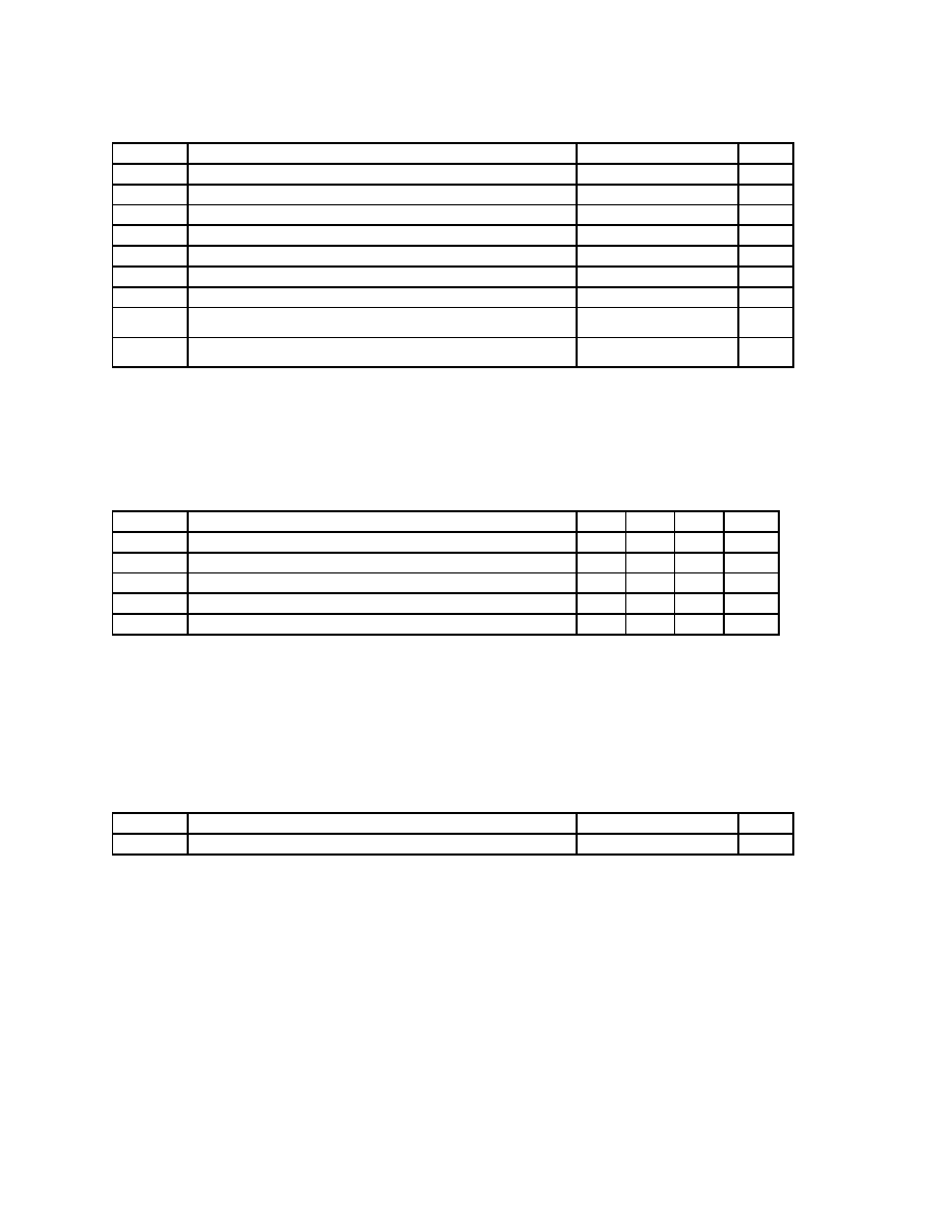
Absolute Maximum Ratings
(Note 1)
SYMBOL PARAMETER
Value
UNITS
V5
5V Power Supply
6
V
V
logic
Input logic level
V5 + 0.3
V
V10
10V Power Supply
12
V
T
STORE
Storage Temperature Range
-55∫ to 150∫
∞C
VPP, VNN Supply Voltage (Note 5)
+/-70
V
T
A
Operating Free-air Temperature Range
-40∫ to 85∫
∞C
T
J
Junction
Temperature
150∫
∞C
ESD
HB
ESD Susceptibility ≠ Human Body Model (Note 2)
All pins
TBD
V
ESD
MM
ESD Susceptibility ≠ Machine Model (Note 3)
All pins
TBD
V
Note 1: Absolute Maximum Ratings indicate limits beyond which damage to the device may occur.
See the table below for Operating Conditions.
Note 2: Human body model, 100pF discharged through a 1.5K
resistor.
Note 3: Machine model, 220pF ≠ 240pF discharged through all pins.
Operating Conditions
(Note 4)
SYMBOL PARAMETER MIN.
TYP.
MAX.
UNITS
V5
5V Power Supply
4.5
5
5.5
V
V10
10V Power Supply
9
10
11
V
T
A
Operating Temperature Range
-40
25
85
∞C
VPP
Positive Supply Voltage (note 5)
15
TBD
V
VNN
Negative Supply Voltage (note 5)
-15
-TBD
V
Note 4: Recommended Operating Conditions indicate conditions for which the device is functional.
See Electrical Characteristics for guaranteed specific performance limits.
Note 5: The supply limitation is based on the internal over-current detection circuit. This limitation is
subject to additional characterization. In addition, depending on feedback configuration, the TDA1400
can be used in single-supply applications, in which case, the negative supply, VNN, is not needed.
Thermal Characteristics
SYMBOL PARAMETER
Value
UNITS
JA
Junction-to-ambient Thermal Resistance (still air)
TBD
C/W

T r i p a t h T e c h n o l o g y, I n c . - P r e l i m i n a r y I n f o r m a t i o n
3
T D A 1 4 0 0 ≠ R e v . 0 . 6 5 / K L i / 0 2 . 0 6
Electrical Characteristics
(Note 6)
T
A
= 25
∞C. See Application/Test Circuit on page 7. Unless otherwise noted, the supply voltages are
V5=5V, V10=10V, and VPP = 60V.
SYMBOL PARAMETER
CONDITIONS MIN.
TYP.
MAX.
UNITS
I
5Q
Quiescent Current
(Mute = 0V)
50
mA
I
10Q
Quiescent Current
(Mute = 0V)
No Load, FETs: FQP19N10,
FQP22P10, R
BBM
= 40.2k
100 mA
I
VPPQ
Quiescent Current
(Mute = 0V)
No Load, FETs: FQP19N10,
FQP22P10, R
BBM
= 40.2k
30 mA
I
5MUTE
Mute Supply Current
(Mute = 5V)
50
mA
I
10MUTE
Mute Supply Current
(Mute = 5V)
0
mA
I
VPPMUTE
Mute Supply Current
(Mute = 5V)
0
mA
V
IH
High-level input voltage (MUTE)
3.5
V
V
IL
Low-level input voltage (MUTE)
1.0
V
V
OH
High-level output voltage (HMUTE) I
OH
= 3mA
4.0
V
V
OL
Low-level output voltage (HMUTE) I
OL
= 3mA
0.5
V
V
TOC
Over Current Sense Voltage
Threshold
XXV Common Mode Voltage
XXV Common Mode Voltage
TBD
TBD
0.56
0.56
TBD
TBD
V
I
VPPSENSE
VPPSENSE Threshold Currents
Over-voltage turn on (muted)
Over-voltage turn off (mute off)
Under-voltage turn off (mute off)
Under-voltage turn on (muted)
TBD
TBD
138
135
55
52
TBD
TBD
µA
µA
µA
µA
V
VPPSENSE
Threshold Voltages with
R
VPP1
= R
VPP1
= 562K
(Notes 7, 8)
Over-voltage turn on (muted)
Over-voltage turn off (mute off)
Under-voltage turn off (mute off)
Under-voltage turn on (muted)
TBD
TBD
77.6
75.9
30.9
29.2
TBD
TBD
V
V
V
V
I
VNNSENSE
VNNSENSE
Threshold
Currents
Over-voltage turn on (muted)
Over-voltage turn off (mute off)
Under-voltage turn off (mute off)
Under-voltage turn on (muted)
TBD
TBD
138
135
51
48
TBD
TBD
µA
µA
µA
µA
V
VNNSENSE
Threshold Voltages with
R
VNN1
= 562K
R
VNN2
= 1.69M
(Note 7, 8)
Over-voltage turn on (muted)
Over-voltage turn off (mute off)
Under-voltage turn off (mute off)
Under-voltage turn on (muted)
TBD
TBD
77.6
75.9
28.7
27.0
TBD
TBD
V
V
V
V
Note 6: Minimum and maximum limits are guaranteed but may not be 100% tested.
Note 7: These supply voltages are calculated using the I
VPPSENSE
and I
VNNSENSE
values shown in the Electrical
Characteristics table. The typical voltage values shown are calculated using a R
VPP
and R
VNN
values without
any tolerance variation. The minimum and maximum voltage limits shown include either a +1% or ≠1% (+1%
for Over-voltage turn on and Under-voltage turn off, -1% for Over-voltage turn off and Under-voltage turn on)
variation of R
VPP
or R
VNN
off the nominal 562kohm and 1.69Mohm values. These voltage specifications are
examples to show both typical and worst case voltage ranges for the given R
VPP
and R
VNN
resistor values.
Please refer to the Application Information section for a more detailed description of how to calculate the over
and under voltage trip voltages for a given resistor value.
Note 8: The fact that the over-voltage specifications exceed the absolute maximum of +/-70V for the TDA1400 does
not imply that the part will work properly at these elevated supply voltages. It also does not imply that the
TDA1400 is tested or guaranteed at these supply voltages. The supply voltages are simply a calculation
based on the process spread of the I
VPPSENSE
and I
VNNSENSE
currents (see note 7). .

T r i p a t h T e c h n o l o g y, I n c . - P r e l i m i n a r y I n f o r m a t i o n
4
T D A 1 4 0 0 ≠ R e v . 0 . 6 5 / K L i / 0 2 . 0 6
Performance Characteristics ≠ Single Supply
T
A
= 25
∞C. Unless otherwise noted, the supply voltages are V5=5V, V10=10V, and VPP = 60V, the input
frequency is 100Hz and the measurement bandwidth is 20kHz. See Application/Test Circuit.
SYMBOL PARAMETER
CONDITIONS MIN.
TYP.
MAX.
UNITS
P
OUT
Output
Power
(continuous output)
THD+N = 0.1%, R
L
= 4
THD+N = 1%, R
L
= 4
THD+N = 10%, R
L
= 4
THD+N = 0.1%, R
L
= 6
THD+N = 1%, R
L
= 6
THD+N = 10%, R
L
= 6
THD+N = 0.1%, R
L
= 8
THD+N = 1%, R
L
= 8
THD+N = 10%, R
L
= 8
310
350
425
240
270
320
180
200
260
W
W
W
W
W
W
W
W
W
THD + N Total Harmonic Distortion Plus
Noise
P
OUT
= 100W, R
L
= 8
0.005 %
IHF-IM IHF
Intermodulation
Distortion 19kHz, 20kHz, 1:1 (IHF), R
L
= 8
P
OUT
= 25W/Channel
0.05 %
SNR Signal-to-Noise
Ratio
A Weighted, R
L
= 4
,
P
OUT
= 425W/Channel
104 dB
Power Efficiency
P
OUT
= 250W/Channel, R
L
= 8
90 %
A
V
Amplifier
Gain
P
OUT
= 10W/Channel, R
L
= 8
See Application / Test Circuit
TBD V/V
A
VERROR
Channel to Channel Gain Error
P
OUT
= 10W/Channel, R
L
= 8
See Application / Test Circuit
0.5
dB
e
NOUT
Output Noise Voltage
A-Weighted, input shorted
R
FBC
= 20k
, R
FBB
= 2.21k
, and
R
FBA
= 1k
250
µV
V
OFFSET
Output Offset Voltage
No Load, Mute = Logic Low
1% R
FBA,
R
FBB
and R
FBC
resistors
-1.0 1.0 V

T r i p a t h T e c h n o l o g y, I n c . - P r e l i m i n a r y I n f o r m a t i o n
5
T D A 1 4 0 0 ≠ R e v . 0 . 6 5 / K L i / 0 2 . 0 6
TDA1400 Pinout
F
BK_
N
E
G
NC
O
C
SN_
N
EG
O
C
SP_
NEG
GA
TE
OF
F
BBM
SET
V5
AGN
D
DC
MP
BI
ASCAP
OA
OU
T
_
A
U
X
NC
NC
NC
HO_POS
AGND
VPPSENSE
NC
VNNSENSE
NC
19
42
41
39
38
40
37
48-pin LQFP
(Top View)
20
21
22
PGND
LO_POS
AGND
24
23
NC
INV_AMP
OAOUT_AMP
V5
V5
48
47
45
44
46
43
MUTE
PGND
HO_NEG
LO_NEG
NC
13
14
15
16
NC
NC
18
17
1
11
10
12
9
8
7
6
5
4
3
2
30 29
27 26
28
25
36 35
33 32
34
31
OC
D1
V1
0
F
BK_
PO
S
NC
OC
S
N
_P
OS
O
C
SP_
PO
S
FA
U
L
T
NC
V5
OC
D2
RE
F
SUB
I
N
V_
AUX