 | –≠–ª–µ–∫—Ç—Ä–æ–Ω–Ω—ã–π –∫–æ–º–ø–æ–Ω–µ–Ω—Ç: TPS4100 | –°–∫–∞—á–∞—Ç—å:  PDF PDF  ZIP ZIP |

Tripath Technology, Inc. ≠ Preliminary Technical Information
1
TPS4100 ≠ KL/Rev. 2.5/02.05
TPS4100
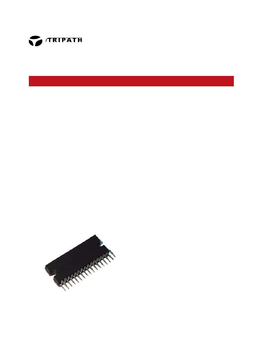
FOUR CHANNEL BRIDGED OUTPUT POWER STAGE
R e v i s i o n 2 . 5 - F e b r u a r y 2 0 0 5
G E N E R A L D E S C R I P T I O N
The TPS4100 is a 4 channel bridged (16 power transistors) output power stage. The TPS4100
accepts 5V CMOS logic signals from a Class-T processor, such as TCD6001, to create a high
fidelity 4 channel audio amplifier. The TPS4100 has been designed specifically for automotive head
unit applications operating on a single 10-26V supply.
A P P L I C A T I O N S
Automotive Head Units and Trunk
Amplifiers
DVD Receivers
Multimedia Speaker Systems
B E N E F I T S
4-channel output stage ≠ with integrated
driver and FETs - in a single 32-pin SSIP
package
Low external component count
Single-supply operation
F E A T U R E S
Four H-Bridge outputs
High Efficiency
High Power @25.0V
100W
sat. sq. wave
@
4
High Efficiency
88% @ 100W 4
AM "Low EMI" mode with connection to
appropriate Class-T controller
Mates seamlessly with TCD6001 Digital Input
Class-T controller
Mute and Stand-By function
Protection Modes:
Output Short to VPP and Ground
Output Short across Load
Load Dump Protection
Over-/Under-Voltage Protection
Over-current Protection
Over-temperature Protection
Fortuitous Open Ground

Tripath Technology, Inc. ≠ Preliminary Technical Information
2
TPS4100 ≠ KL/Rev. 2.5/02.05
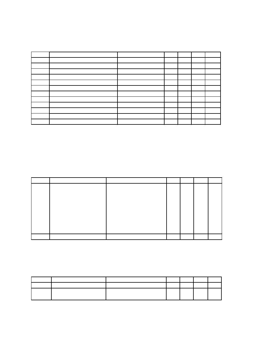
Absolute Maximum Ratings
(Notes 1, 2)
SYMBOL PARAMETER
Value
UNITS
VPP
Supply Voltage (VPP) 33
V
VPP
MAX
Peak Supply Voltage (t<50ms) 60
V
VIN
RANGE
Voltage Range for Input Section Pins (Note 2)
Inputs (Pins 1-11)
-0.5 to 5.5
V
T
STORE
Storage Temperature Range
-55 to +150
∫C
I
R
Repetitive Peak Output Current
12
A
Tj
Maximum Junction Temperature
150
∫C
P
D
Total Power Dissipation
(Tcase = 70∫C)
80
W
ESD
ESD Susceptibility - Human Body Model (Note 3)
2k
V
ESD
ESD Susceptibility ≠ Machine Model (Note 4)
200
V
Note 1: Absolute Maximum Ratings indicate limits beyond which damage to the device may occur.
See the table below for Operating Conditions.
Note 2: The input section pins (pins 1-11) should not be connected to voltages over 5.5V with respect to pins 13 and 14
(AGND). Please note that pin 12 is an output and can be damaged if a voltage is forced externally.
Note 3: Human body model, 100pF discharged through a 1.5K
resistor.
Note 4: Machine model, 220pF ≠ 240pF discharged through all pins.
Operating Conditions
(Note 5)
SYMBOL PARAMETER MIN.
TYP.
MAX.
UNITS
VPP
Supply Voltage (Note 5)
10
14.4
26
V
T
A
Operating Free Air Temperature Range
-40
25
85
∫C
Note 5: Recommended Operating Conditions indicate conditions for which the device is functional.
See Electrical Characteristics for guaranteed specific performance limits.
Thermal Characteristics
SYMBOL PARAMETER
Value
UNITS
JC
Junction-to-case Thermal Resistance
1.0
∞
C/W
JA
Junction-to-ambient Thermal Resistance (still air)
20
∞
C/W

Tripath Technology, Inc. ≠ Preliminary Technical Information
3
TPS4100 ≠ KL/Rev. 2.5/02.05
Electrical Characteristics
(Note 6)
T
A
= 25
∞C. Unless otherwise noted, the supply voltage is VPP=14.4V. See Application/Test Circuit.
Note 6: Minimum and maximum limits are guaranteed but may not be 100% tested.
Performance Characteristics
(Note 6)
T
A
= 25
∞C. Unless otherwise noted, R
L
= 4
. Measurement Bandwidth = 20kHz. All specifications
shown are applicable only when the TPS4100 is used in conjunction with the TCD6001 Class-T
Controller. See Application/Test Circuit of TCD6001 data sheet for additional information.
AM Mode
(Note 6)
T
A
= 25
∞C. Unless otherwise noted, the supply voltage is VPP=14.4V, R
L
= 4
. Measurement
Bandwidth = 20kHz. See Application/Test Circuit.
.
Note 7: The TPS4100 heat sinking in AM Mode must be increased (as compared to Class-T mode) to sustain the
typical output numbers. This is due to the lower efficiency of Class B output stage operation.
SYMBOL PARAMETER
Conditions
MIN.
TYP.
MAX.
UNITS
I
STBY
Stand-By Current
V
SLEEPB
< 0.15V
100
200
µA
V
IL
Stand-By On Threshold Voltage
SLEEPB Low (amp off)
0.6
V
V
IH
Stand-By Off Threshold Voltage
SLEEPB High (amp on)
2.3
V
V
IL
Mute-On Threshold Voltage
MUTE Low
1
V
V
IH
Mute-Off Threshold Voltage
MUTE High
2.3
V
V
IL
Yn/YnB Low Threshold Voltage
0.6
V
V
IH
Yn/YnB High Threshold Voltage
2.3
V
V
OH
Fault Reporting Logic Output High Voltage Open Drain Output
3.5
V
V
OL
Fault Reporting Logic Output Low Voltage
R
FAULT
= 51K
1 V
V
IH
AM Mode On Threshold Voltage
2.3
V
V
IL
AM Mode Off Threshold Voltage
1
V
I
AM
AM Mode Pin Input Current
1
µA
SYMBOL PARAMETER
CONDITIONS MIN.
TYP.
MAX.
UNITS
P
OUT
Output
Power
(Continuous power/ channel)
VPP=25V saturated sq. wave
VPP=25V THD+N=10%
VPP=25V THD+N=1%
VPP=20V saturated sq. wave
VPP=20V THD+N=10%
VPP=20V THD+N=1%
VPP=14.4V sat. sq. wave, R
L
= 2
VPP=14.4V THD+N=10%, R
L
= 2
VPP=14.4V THD+N=1%, R
L
= 2
VPP=14.4V saturated sq. wave
VPP=14.4V THD+N=10%
VPP=14.4V THD+N=1%
95
65
35
112
80
65
74
51
40
63
42
33
39
26
21
W
W
W
W
W
W
W
W
W
W
W
W
Power Efficiency
VPP=25V, 4 x 100W sat sq wave
84
88
%
SYMBOL PARAMETER
CONDITIONS MIN.
TYP.
MAX.
UNITS
I
OCD
Over-current
detect
5.5
A
Pout
Output Power (Note 7)
VPP=16V, THD+N=10%
VPP=14.4V, THD+N=10%
13
20
16
W
W

Tripath Technology, Inc. ≠ Preliminary Technical Information
4
TPS4100 ≠ KL/Rev. 2.5/02.05
Protection Circuits
(Note 5)
T
A
= 25
∞C. Unless otherwise noted, the supply voltage is VPP=14.4V.
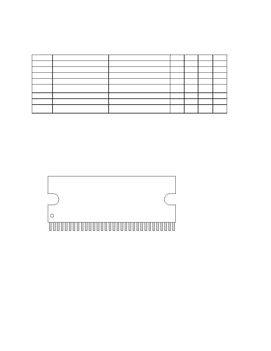
TPS4100 Pinout
32-pin SSIP Package
(Top
view)
OUT1P
CP
UMP
PGN
D
OUT4N
OUT3N
VPP3
OUT3P
FAULT
OUT2P
VPP2
OUT2N
SLEEPB
OUT1N
PGN
D
VPP1
DCA
P
OUT4P
AGN
D
AGN
D
V5GEN
AM
MUTE
B
Y4B
Y4
Y3B
Y3
Y2
Y1B
Y1
PGN
D
VPP4
Y2B
30
16
17
18
19
20
21
22
23
24
25
26
27
28
29
1
15
14
13
11
10
12
9
8
7
6
5
4
3
2
32
31
Note: The heat slug of the TPS4100 is connected to PGND.
SYMBOL PARAMETER
CONDITIONS MIN.
TYP.
MAX.
UNITS
OV
ON
Over-voltage
Threshold
Over-voltage turn on (amp muted)
27.0
30
32.5
V
OV
OFF
Over-voltage
Reset
Over-voltage
turn off (mute off)
26.0
28.0
V
UV
OFF
Under-voltage Reset
Under-voltage turn off (mute off)
9.5
10.0
V
UV
ON
Under-voltage
Threshold
Under-voltage turn on (amp muted)
7.8
8.1
8.6
V
OT
ON
Over-Temperature
Threshold
Over-temperature turn on (amp
muted)
150
160 170
∞C
OT
OFF
Over-Temperature Reset
Over-temperature turn off (mute off)
120
130 140
∞C
I
OC
Over-Current Detect
Single cycle, 1kHz input ramp
8.0
9.5
A
VP
MAX
Load Dump Voltage Withstand
Test conditions, t
r
> 2.5ms,
t
pulse
<50mS
60 V

Tripath Technology, Inc. ≠ Preliminary Technical Information
5
TPS4100 ≠ KL/Rev. 2.5/02.05
TPS4100 Pinout
PIN NAME/FUNCTION
TYPE DESCRIPTION
1
SLEEPB
INPUT (L) Logic input, ACTIVE LOW. Setting SLEEP to low puts the TPS4100 in sleep
mode. Input range is 0 to 5V with 3.3V compliant inputs.
2, 4, 6, 8
Y1, Y2, Y3, Y4
INPUT (L) Non-inverted switching modulator inputs.
3, 5, 7, 9
Y1B, Y2B, Y3B, Y4B
INPUT (L) Inverted switching modulator inputs.
10
MUTEB
INPUT (L) Logic Input, ACTIVE LOW. Setting MUTE to low puts the device in mute mode.
Typically driven by external power supply or microcontroller. Input range is 0 to
5V with 3.3V compliant inputs.
11
AM
INPUT (L) Logic input, ACTIVE HIGH. Enables Analog Mode operation. Typically driven
by Tripath controller. Input range is 0 to 5V with 3.3V compliant inputs.
12
5VGEN
OUTPUT On chip 5V regulator bypass capacitor connection
12
HMUTEB
OUTPUT (L) Logic output, ACTIVE LOW. HMUTEB low indicates TPS4100 is in mute mode
13, 14
AGND
GND
Analog ground
15 CPUMP
OUTPUT
Charge pump output capacitor
16
OUT4P
OUTPUT Positive Output Channel 4
17
VPP4
POWER Positive Supply Voltage Channel 4
18
PGND
GND
Power Ground for Outputs 3 and 4
19
OUT4N
OUTPUT Negative Output Channel 4
20
OUT3N
OUTPUT Negative Output Channel 3
21
VPP3
POWER Positive Supply Voltage Channel 3
22
OUT3P
OUTPUT Positive Output Channel 3
23
FAULT
OUTPUT (L) Open Drain Logic Output, ACTIVE HIGH. FAULT high indicates fault condition.
24
OUT2P
OUTPUT Positive Output Channel 2
25
VPP2
POWER Positive Supply Voltage Channel 2
26
OUT2N
OUTPUT Negative Output Channel 2
27
OUT1N
OUTPUT Negative Output Channel 1
28
PGND
GND
Power Ground for Outputs 1 and 2
29
VPP1
POWER Positive Supply Voltage Channel 1
30
OUT1P
OUTPUT Positive Output Channel 1
31
DCAP
OUTPUT Oscillator output for driving external charge pump circuit
32 PGND GND
Power
Ground
