 | –≠–ª–µ–∫—Ç—Ä–æ–Ω–Ω—ã–π –∫–æ–º–ø–æ–Ω–µ–Ω—Ç: 1340 | –°–∫–∞—á–∞—Ç—å:  PDF PDF  ZIP ZIP |

1340-Type Receiver Lightwave Receiver
Data Sheet
February 2003
TriQuint Optoelectronics
Operating at 1.1
µm through 1.6 µm wavelengths and at
155 Mb/s, 622 Mb/s, or 1.25 Gb/s, the versatile 1340-Type
Receiver is manufactured in a 20-pin, plastic DIP with a multi-
mode fiber pigtail.
Features
Backward compatible with 1310 receiver family
Space-saving, self-contained, 20-pin plastic DIP
Silicon based ICs
Single 5 V power supply operation including photo-
current monitor capability
Exceeds all SONET (GR-253-CORE) and ITU-T
G.958 jitter requirements
Wide dynamic range
Qualified to meet the intent of Telcordia Technologies
*
reliability practices
Operates at data rates of 155 Mb/s,
622 Mb/s, or 1.25 Gb/s
Positive ECL (PECL) data outputs
CMOS (TTL) link-status flag output
Operation at 1.3
µm or 1.55 µm wavelengths
Operating case temperature range of
≠40 ∞C to +85 ∞C
Applications
Telecommunications
-- Inter- and intraoffice SONET/ITU-T SDH
-- Subscriber loop
-- Metropolitan area networks
High-speed data communications
Description
The 1340-Type receiver is designed for use in trans-
mission systems or medium- to high-speed data com-
munications applications at data rates up to 1.25 Gb/s.
Compact packaging, along with wide dynamic range,
makes these receivers ideal for both telecommunica-
tions and data communications applications.
The following three versions of the receiver are avail-
able:
SONET/SDH compliant with OC-3/STM-1
SONET/SDH compliant with OC-12/STM-4
1.25 Gbits for data applications.
* Telcordia Technologies is a trademark of Telcordia Technologies
Inc.
x134
0 622
MB
Æ
riQ
T
uint
SEMIC
ONDU
CTOR
1340-T
ype R
eceive
r

2
2
For additional information and latest specifications, see our website: www.triquint.com
Data Sheet
February 2003
1340-Type Lightwave Receiver
Description
(continued)
The SONET/SDH versions of the receiver are fully
compliant with the latest issue of Telcordia Technolo-
gies GR-253- CORE and the most recent issues of ITU
recommendations G.957 and G.958. The 1340-Type
receiver requires only a single 5 V power supply for
operation. All versions of the receiver are characterized
for operation over the case operating range of ≠40 ∞C
to +85 ∞C at the appropriate data rate for each version.
Manufactured in a 20-pin DIP, the receivers use a pla-
nar, rear illuminated InGaAs PIN photodetector that
allows these receivers to be used at wavelengths from
1.1 µm to 1.6 µm. The photocurrent output of the PIN
detector is amplified and converted to a voltage by a
silicon amplifier. A silicon quantizer provides additional
signal amplification, data threshold detection, and
PECL data outputs. The incoming optical signal is cou-
pled into the receiver through a 62.5 µm core multi-
mode fiber pigtail. The outer jacket diameter of the
pigtail is 900 µm. The receiver can be ordered with the
pigtail terminated in an FC/PC, SC, or ST
Æ
optical con-
nector. Other connectors are available on special
order. See your TriQuint account representative for
ordering conditions and information.
The receiver has differential PECL data outputs and,
depending on the version selected, either differential
PECL link status flag or complementary CMOS link sta-
tus flag outputs. The link status flag outputs indicate
the presence or absence of a minimum acceptable
level of optical input signal.
1-414(C)
Figure 1. Block Diagram

Data Sheet
1340-Type Lightwave Receiver
February 2003
For additional information and latest specifications, see our website: www.triquint.com
3
Description
(continued)
To help ensure high product reliability and customer
satisfaction, TriQuint is committed to an intensive qual-
ity program that starts in the design phase and pro-
ceeds through the manufacturing and shipping pro-
cess. Optoelectronics subsystems are qualified to
TriQuint internal standards using MIL-STD-883 test
methods and pro-cedures and sampling techniques
consistent with Telcordia Technologies requirements.
The 1340 receiver qualification program meets the
intent of Telcordia Technologies TR-NWT-000468 and
TA-TSY-000983.
Application Information
The 1340 receiver is a highly sensitive fiber-optic
receiver. Although the data outputs are digital logic lev-
els (PECL), the device should be thought of as an ana-
log component. When laying out the printed-wiring
board (PWB), the 1340 receiver should be given the
same type of consideration one would give to a sensi-
tive analog component.
At a minimum, a double-sided printed-wiring board with
a large component-side ground plane beneath the
receiver must be used. In applications that include
many other high-speed devices, a multilayer PWB is
highly recommended. This permits the placement of
power and ground connections on separate layers,
which helps minimize the coupling of unwanted signal
noise into the power supplies of the receiver.
Layout Considerations
A fiber-optic receiver employs a very high-gain, wide-
bandwidth transimpedance amplifier. The amplifier
detects and amplifies signals that are only tens of nA in
amplitude. Any unwanted signal currents that couple
into the receiver circuitry cause a decrease in the
receiver's sensitivity and can also degrade the perfor-
mance of the receiver's loss of signal (FLAG) circuit.
To minimize the coupling of unwanted noise into the
receiver, route high-level, high-speed signals such as
transmitter inputs and clock lines as far away as possi-
ble from the receiver pins. If this is not possible, then
the PWB layout engineer should consider interleaving
the receiver signal and flag traces with ground traces in
order to provide the required isolation.
Noise that couples into the receiver through the power
supply pins can also degrade device performance. The
application schematics, Figures 3--5, show recom-
mended power supply filtering that helps minimize
noise coupling into the receiver. The bypass capacitors
should be high-quality ceramic devices rated for RF
applications. They should be surface-mount compo-
nents placed as close as possible to the receiver power
supply pins. The ferrite bead should have as high an
impedance as possible in the frequency range that is
most likely to cause problems. This will vary for each
application and is dependent on the signaling frequen-
cies present on the application circuit card. Surface-
mount, high-impedance beads are available from sev-
eral manufacturers.
Data and Flag Outputs
The data outputs of the 1340 receiver are driven by
open-emitter NPN transistors which have an output
impedance of approximately 7
. Each output can pro-
vide approximately 50 mA maximum output current.
Due to the high switching speeds of ECL outputs,
transmission line design must be used to interconnect
components. To ensure optimum signal fidelity, both
data outputs (DATA and DATA) should be terminated
identically. The signal lines connecting the data outputs
to the next device should be equal in length and should
have matched impedances.
Controlled impedance stripline or microstrip construc-
tion must be used to preserve the quality of the signal
into the next component and to minimize reflections
back into the receiver. Excessive ringing due to reflec-
tions caused by improperly terminated signal lines
makes it difficult for the component receiving these sig-
nals to decipher the proper logic levels and may cause
transitions to occur where none were intended. Also,
by minimizing high frequency ringing due to reflections
caused by improperly designed and terminated signal
lines, possible EMI problems can be avoided. The
applications sections in the Signetics
*
ECL 10K/100K
Data Manual or the National Semiconductor
ECL
Logic Databook and Design Guide provide excellent
design information on ECL interfacing.
* Signetics is a registered trademark of Signetics Corp.
National Semiconductor is a registered trademark of National
Semiconductor Corporation.

4
4
For additional information and latest specifications, see our website: www.triquint.com
Data Sheet
February 2003
1340-Type Lightwave Receiver
Data and Flag Outputs
(continued)
The FLAG and FLAG outputs of the OC-3/STM-1
155 Mb/s version of the 1340 receiver are PECL logic
levels driven by open emitter transistors with the same
characteristics as the data outputs. These out-puts
must be properly terminated in order to obtain the cor-
rect logic levels. Since the FLAG function is basically a
dc switch that indicates the loss of optical input signal,
it can be interfaced to much slower TTL or CMOS logic
circuits.
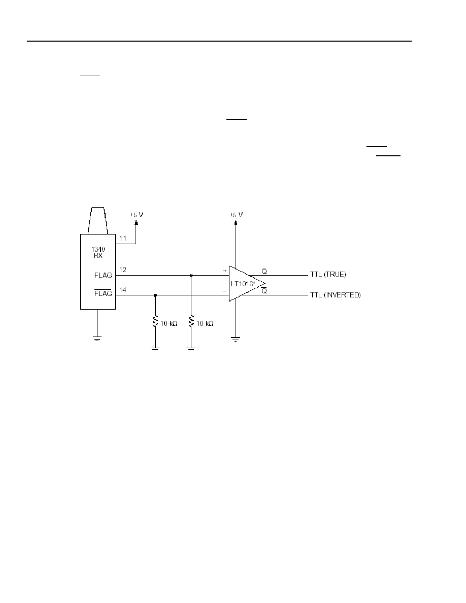
The circuit shown in Figure 2 provides one example of
how to create a TTL logic output from the PECL FLAG
output signal. The outputs of the LT1016 are TTL-com-
patible and provide both true and inverted logic levels.
The Q output of this circuit will be a TTL high (>2.5 V)
when the 1340 is receiving an optical signal greater
than the FLAG switching threshold and will be a TTL
low (<0.4 V) whenever the optical signal is absent or is
below the FLAG switching threshold. The FLAG and
FLAG outputs of the OC-12/STM-4 and 1.25 Gb/s
receivers are 5 V TTL logic level compatible. The FLAG
output is provided directly by the comparator IC. How-
ever, the FLAG output is derived from the FLAG output
through an inverter. Excessive loading of the FLAG
output can cause the FLAG output to malfunction.
1-800(C).a
* Part available from Linear Technology Corporation of Milpitas, CA 95035.
Figure 2. Converting PECL FLAG Outputs to TTL

For additional information and latest specifications, see our website: www.triquint.com
5
Data Sheet
1340-Type Lightwave Receiver
February 2003
Pin 10
Pin 10 on the 1340-Type receiver is a not internally
connected (NIC) pin. This definition allows the 1340 to
be used in most customer 20-pin receiver module
applications. Customer's printed-wiring boards that are
designed with ground, +5 V, ≠5 V, or no connection to
this pin are all acceptable options. For those applica-
tions that require monitoring the photocurrent of the
PIN photodetector for power monitoring purposes,
there are versions of the 1340 that require +5 V or ≠5 V
applied to Pin 10. Check Tables 4 and 5 for ordering
information.
Recommended User Interface
The 1340 receiver is designed to be operated from a
5 V power supply and provides raised or pseudo-ECL
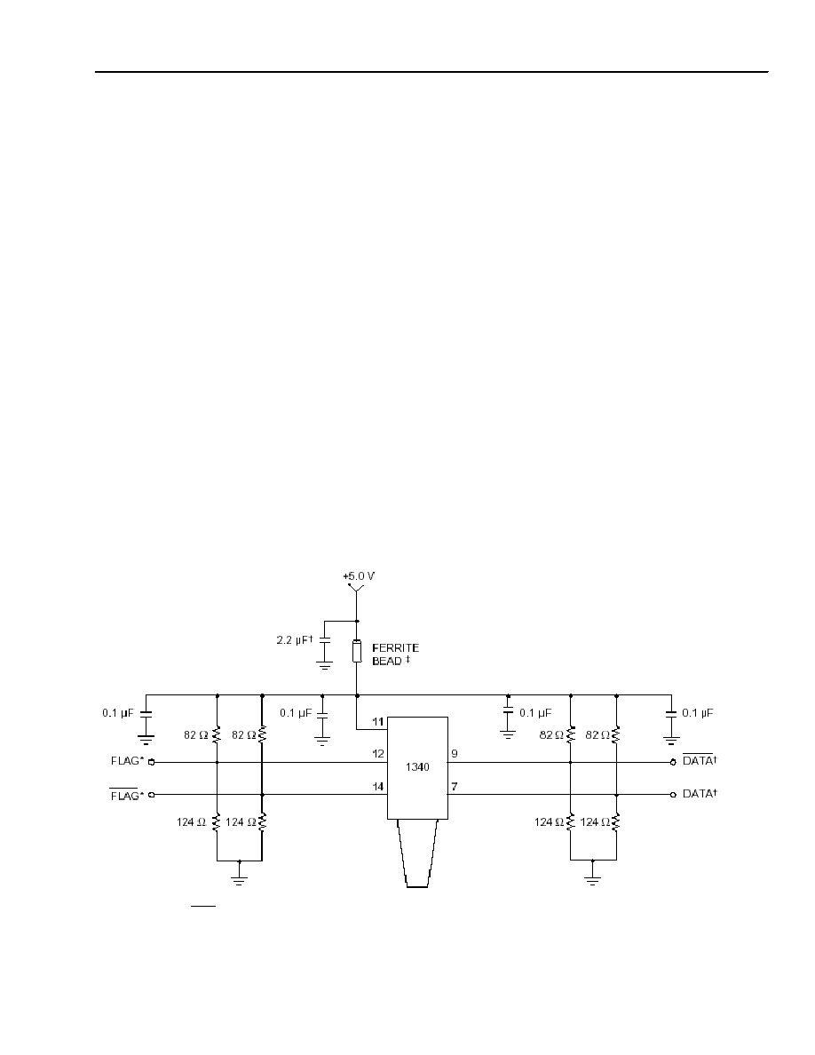
(PECL) data outputs. Figures 3 and 4 show two possi-
ble application circuits for the 1340 receiver. Figure 3
represents an application for the version with PECL
FLAG outputs while Figure 4 shows a possible applica-
tion for the version with the TTL-compatible FLAG
outputs.
In both instances, the DATA outputs are terminated
with a ThÈvenin equivalent circuit, which provides the
equivalent of a 50
load terminated to (V
CC
≠ 2 V).
A single 50
resistor terminated to (V
CC
≠ 2 V) could
also be used, but this requires a second power supply.
Other methods of terminating ECL-type outputs are
discussed in the references previously mentioned.
Figure 5 shows an example of a circuit that can be
used to interface the PECL outputs of the 1340
receiver with a device which requires true, negative
voltage ECL inputs. The 100314 is an ECL line receiver
and is shown here only as an example to demonstrate
this coupling procedure. The DATA lines are terminated
in a 50
equivalent impedance but are ac-coupled to
the 100314. The capacitive coupling isolates and per-
mits level shifting of the positive DATA outputs of the
receiver to the proper negative level required by the
inputs of the 100314. The V
BB
output of the 100314
provides the reference voltage required to center the
voltage swing of the DATA signals around the input
switching threshold of the 100314. The ThÈvenin
equivalent of the 166
and 250 resistor pair is
100
, which, in parallel with the 100 resistor con-
nected to V
BB
, results in a 50
equivalent impedance
for the load on each of the data lines. Alternatively, if
there is no V
BB
reference available, a second pair of
166
/250 resistor networks could be used on the
data lines on the 100314 side of the coupling capacitor.
* 50
to (V
CC
≠ 2) V.
DATA and
DATA
are 50
impedance transmission lines; both lines can be ac- or dc-coupled into the next device.
Fair-Rite Products Corporation part number 2743037447 or equivalent.
Note: All unused outputs must be terminated as shown. All resistors are 1/8 W, thin-film, ceramic chips. All capacitors are
25 Vdc, ceramic X7R, or equivalent.
Figure 3. Interfacing to the 155 Mb/s 1340 Receiver
1-500(C).d

6
For additional information and latest specifications, see our website: www.triquint.com
Data Sheet
February 2003
1340-Type Lightwave Receiver
Recommended User Interfaces
(continued)
* TTL (CMOS) compatible level.
DATA and DATA are 50
impedance transmission lines; both lines can be ac- or dc-coupled into the next device.
Fair-Rite Products Corporation part number 2743037447 or equivalent.
Figure 4. Interfacing to the 622 Mb/s and 1.25 Gb/s 1340 Receivers
1-572(C).b
* 50
to (V
CC
≠ 2) V.
50
to ≠2 V. DATA and DATA are 50 impedance transmission lines.
Fair-Rite Products Corporation part number 2743037447 or equivalent.
Figure 5. Interfacing the 155 Mb/s 1340 Receiver to a True ECL Circuit
1-500(C).c

Data Sheet
1340-Type Lightwave Receiver
February 2003
For additional information and latest specifications, see our website: www.triquint.com
7
Pin Information
Table 1. Pin Descriptions
* Pins designated as no user connection are not connected internally
within the receiver. However, to allow for future functional
upgrades, it is recommended that the user not make any connec-
tions to these pin positions.
The link-status flag is a logic output that indicates the presence or
absence of a minimum acceptable level of optical input. A logic
high on FLAG indicates the presence of a valid optical signal.
Handling Precautions
Mounting and Connections
The pigtail consists of a 39 in. ± 4 in. (1 m ± 10 cm),
62.5 µm core/125 µm cladding multimode fiber. The
standard fiber has a 0.036 in. (914 µm) diameter tight-
buffered outer jacket. The minimum fiber bending
radius during operation is 1.0 in. (25.4 mm).
Electrostatic Discharge
CAUTION: This device is susceptible to damage as
a result of electrostatic discharge. Take
proper precautions during both handling
and testing. Follow EIA* standard EIA-
625.
TriQuint Semiconductor employs a human-body model
(HBM) for ESD-susceptibility testing and protection-de-
sign evaluation. ESD voltage thresholds are dependent
on the critical parameters used to define the model. A
standard HBM (resistance = 1.5 k
, capacitance =
100 pF) is widely used and can be used for comparison
purposes. The HBM ESD withstand voltage established
for the 1340-type transmitter is ± 1000 V.
Receiver Processing
The 1340-type receiver devices can withstand normal
wave-soldering processes. The complete receiver
module is not hermetically sealed; therefore, it should
not be immersed in or sprayed with any cleaning solu-
tion or solvents. The process cap and fiber pigtail
jacket deformation temperature is 85 ∞C. The receiver
pins can be wave-soldered at maximum temperature of
250 ∞C for 10 seconds.
Installation Considerations
Although the receiver features a robust design, care
should be used during handling. The optical connector
should be kept free from dust, and the process cap
should be kept in place as a dust cover when the
device is not connected to a cable. If contamination is
present on the optical connector, the use of canned air
with an extension tube should remove any debris.
Other cleaning procedures are identified in the techni-
cal note, Cleaning Fiber-Optic Assemblies (TN95-
010LWP).
* EIA is a registered trademark of Electronic Industries Association.
Pin Number
Description
1
Ground
2
Ground
3
Ground
4
Ground
5
No User Connection*
6
Ground
7
DATA
8
Ground
9
DATA
10
NIC or Optional V
PIN
11
Vcc (5 V)
12
FLAG
13
Ground
14
FLAG
15
Ground
16
Ground
17
No User Connection*
18
No User Connection*
19
No User Connection*
20
No User Connection*

8
For additional information and latest specifications, see our website: www.triquint.com
Data Sheet
February 2003
1340-Type Lightwave Receiver
Absolute Maximum Ratings
Stresses in excess of the absolute maximum ratings can cause permanent damage to the device. These are abso-
lute stress ratings only. Functional operation of the device is not implied at these or any other conditions in excess
of those given in the operations section of the data sheet. Exposure to absolute maximum ratings for extended
periods can adversely affect device reliability.
Operating Characteristics
Minimum and maximum values specified over operating case temperature range and end-of-life (EOL).
Typical values are measured at beginning-of-life (BOL) room temperature unless otherwise noted.
Table 2. Optical Characteristics
* For 1 x 10
≠10
BER with an optical input using a 2
23
≠ 1 pseudorandom word having a 50% average duty cycle.
Parameter
Symbol
Min
Max
Unit
Supply Voltage
V
CC
--
5.5
V
Operating Case Temperature Range
T
C
≠40
85
∞C
Storage Case Temperature Range
T
stg
≠40
85
∞C
Lead Soldering Temperature/Time
--
--
250/10
∞C/s
Operating Wavelength Range
1.1
1.6
µm
Minimum Fiber Bend Radius
--
1.0 (25.4)
--
in. (mm)
Parameter
Symbol
Data Rate
(Mb/s)
Min
Typ
*
Max
Unit
Measured Average Sensitivity
*
P
R
155
622
1250
--
--
--
≠38
≠32
≠28
≠36
≠29
≠24
dBm
dBm
dBm
Maximum Input Power
*
P
MAX
155
622
1250
≠3.0
≠6.0
≠3.0
0
≠3.0
≠2.0
--
--
--
dBm
dBm
dBm
Link Status Switching Threshold:
Decreasing Light Input
Increasing Light Input
Hysteresis
LST
D
LST
I
HYS
155
622
1250
155
622
1250
All Data
Rates
≠53.0
≠45.0
≠36.0
≠52.5
≠45.5
≠35.5
0.5
≠40
≠34
≠31.0
≠38
≠31
≠29.0
3.0
≠36.0
≠28.0
≠26.0
≠35.5
≠27.5
≠25.5
6.0
dBm
dBm
dBm
dBm
dBm
dBm
dBm
Detector Responsivity
R
All Data
Rates
0.7
0.8
1.2
A/W

For additional information and latest specifications, see our website: www.triquint.com
9
Data Sheet
1340-Type Lightwave Receiver
February 2003
Operating Characteristics
(continued)
Table 3. Electrical Characteristics
* Customers have the option for either a +5 V or ≠5 V supply.
Measured from V
CC
with a 50
load to (V
CC
≠ 2) V.
Internally terminated CMOS output.
Qualification Tests and Reliability
To help ensure high product reliability and customer satisfaction, TriQuint is committed to an intensive quality pro-
gram that starts in the design phase and proceeds through the manufacturing process. Optoelectronics modules
are qualified to TriQuint internal standards using MIL-STD-883 test methods and procedures and using sampling
techniques consistent with Telcordia Technologies
requirements. The 1340-Type receivers have undergone an
extensive and rigorous set of qualification tests. This qualification program fully meets the intent of Telcordia Tech-
nologies
reliability practices TR-NWT-000468 and TA-NWT-000983. In addition, the design, development, and
manufacturing facility of the Optoelectronics unit at TriQuint has been certified to be in full compliance with the lat-
est ISO
*-9001 Quality System Standards.
* ISO is a registered trademark of The International Organization for Standardization.
Parameter
Symbol
Min
Typ
Max
Unit
dc Power Supply Voltage
V
CC
4.75
5.0
5.25
V
PIN Photodetector Supply Voltage (Pin 10)*
V
PIN
V
PIN
4.75
≠5.25
5.0
≠5.0
5.25
≠4.75
V
V
Power Supply Current
I
CC
I
PIN
--
--
80
--
150
1
mA
mA
Output Data Voltage:
Low
High
V
OL
V
OH
V
CC
≠ 1.81
V
CC
≠1.025
V
CC
≠ 1.70
V
CC
≠ 0.95
V
CC
≠ 1.62
V
CC
≠ 0.88
V
V
Output Rise Time/Fall Time:
OC-3/STM-1 Versions
OC-12/STM-4 Versions
t
R
/t
F
t
R
/t
F
--
--
700
350
1400
400
ps
ps
Output Flag Voltage:
OC-3/STM-1 Versions:
Low
High
OC-12/STM-4 Versions:
Low
High
V
FL
V
FH
V
FL
V
FH
--
V
CC
≠ 1.025
0
V
CC
≠ 0.5
V
CC
≠ 1.90
V
CC
≠ 1.0
--
--
V
CC
≠ 1.65
--
0.5
V
CC
V
V
V
V
Output Data Current:
Low
High
I
OL
I
OH
--
--
5
20
50
50
mA
mA
Output Flag Current:
OC-3/STM-1 Versions:
Low
High
OC-12/STM-4 Versions:
Low
High
I
OL
I
OH
I
OL
I
OH
--
--
0
0
5
20
10
10
50
50
15
15
mA
mA
mA
mA

10
For additional information and latest specifications, see our website: www.triquint.com
Data Sheet
February 2003
1340-Type Lightwave Receiver
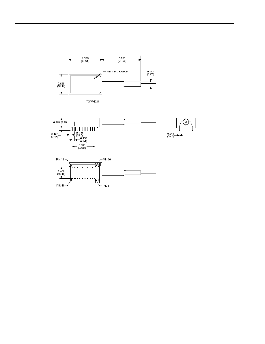
Outline Diagram
Dimensions are in inches and (millimeters). Unless noted otherwise, tolerances are 0.005 in. (0.127 mm).
1-988(C)

Additional Information
For the latest specifications, additional product information, worldwide sales and distribution locations, and information about TriQuint:
Web: www.triquint.com
Tel: (503) 615-9000
E-mail: info_opto@tqs.com
Fax: (503) 615-8902
For technical questions and additional information on specific applications:
E-mail: info_opto@tqs.com
The information provided herein is believed to be reliable; TriQuint assumes no liability for inaccuracies or omissions. TriQuint assumes no responsibility for the use of this information, and all
such information shall be entirely at the user's own risk. Prices and specifications are subject to change without notice. No patent rights or licenses to any of the circuits described herein are
implied or granted to any third party.
TriQuint does not authorize or warranty any TriQuint product for use in life-support devices and/or systems.
Copyright © 2003 TriQuint Semiconductor Inc. All rights reserved.
DS00-098 Revision 1.1, February, 2003
Data Sheet
February 2003
1340-Type Lightwave Receiver
Ordering Information
Table 4. OC-3/STM-1 Receiver Versions
Table 5. OC-12/STM-4 Receiver Versions
Table 6. 1.25 Gb/s Receiver Versions
Table 7. Related Products
Device Code
Connector
Pin 10 Requirements
Comcode
1340FMPC
FC-PC
No
Internal
Connection
108162322
1340CMPC
SC
108354408
1340TMPC
ST
108572264
1340FAPC
FC-PC
Requires +5 V or ≠5 V
(Used for photocurrent
monitoring)
108468687
1340CAPC
SC
108359175
1340TAPC
ST
108572249
Device Code
Connector
Pin 10 Requirements
Comcode
1340FNPC
FC-PC
No
Internal
Connection
108155680
1340CNPC
SC
108354416
1340TNPC
ST
108155755
1340FBPC
FC-PC
Requires +5 V or ≠5 V
(Used for photocurrent
monitoring)
108155672
1340CBPC
SC
108468679
1340TBPC
ST
108572256
Device Code
Connector
Pin 10 Requirements
Comcode
1340FCPC
FC-PC
Requires
+5 V or ≠5 V
108400342
1340CCPC
SC
108400334
Description
Document Number
1241/1243/1245-Type Receivers for SONET/SDH Applications
DS99-228
1345-Type Receiver with Clock Recovery and Data Retiming
DS00-099


