 | –≠–ª–µ–∫—Ç—Ä–æ–Ω–Ω—ã–π –∫–æ–º–ø–æ–Ω–µ–Ω—Ç: 856079 | –°–∫–∞—á–∞—Ç—å:  PDF PDF  ZIP ZIP |
Data Sheet
Part Number 856079
1842.5 MHz SAW Filter
Subject to change or obsolescence without notice
Rev D
05-Sep-2002
Page 1 of 7
Features
∑ For DCS applications
∑ Usable bandwidth 75 MHz
∑ Low loss
∑ High attenuation
∑ Single-ended input
∑ Balanced output
∑ Superior amplitude and phase balance
∑ Ceramic Surface Mount Package (SMP)
∑ Small size
∑
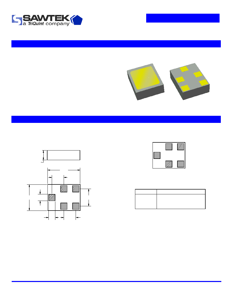
Package
Pin Configuration
Surface Mount 2.50 x 2.00 x 0.76 mm
Bottom View
5
4
3
2
1
Pin No. Description
1
Input
2,5
Case
ground
3,4
Balanced
output
0.76 NOM.
0.84 MAX.
0.50
0.50
2.00
2.50
0.94
1.38
0.94
Dimensions shown are nominal in millimeters
All tolerances are
±0.10mm
Body: Al
2
O
3
ceramic
Lid: Kovar or Alloy 42, Au over Ni plated
Terminations: Au plating 0.5 - 1.0
µm,
over a 2 - 6
µm Ni plating
Data Sheet
Part Number 856079
1842.5 MHz SAW Filter
Subject to change or obsolescence without notice
Rev D
05-Sep-2002
Page 2 of 7
Electrical Specifications
(1)
Operating Temperature:
(2)
+25
o
C
Parameter
(3)
Minimum
Typical
Maximum
Unit
Center Frequency
- 1842.5 -
MHz
Maximum Insertion Loss
1805
-
1880
MHz
-
2.5
2.9
dB
Absolute Attenuation
DC - 1000 MHz
1000 - 1710 MHz
1710
-
1765
MHz
1765
-
1785
MHz
1920 - 1980 MHz
1980 - 2090 MHz
2090
-
3000
MHz
3000
-
6000
MHz
40
30
20
12
15
20
30
40
45
34
25
17
17
27
40
50
-
-
-
-
-
-
-
-
dB
dB
dB
dB
dB
dB
dB
dB
Passband Ripple
(4)
1805
-
1880
MHz
-
0.7
1.0
dB
Input/Output Return Loss
1805
-
1880
MHz
8
10
-
dB
Output Amplitude Balance (|S
31
/S
21
|)
1805
-
1880
MHz
-
1.4
2
dB
Output Phase Balance
(S
31
)-
(S
21
)
1805
-
1880
MHz
165
180
190
degree
Source Impedance
- 50 -
Optimal Load Impedance (balanced)
(5)
-
200 || 18nH
-
Notes:
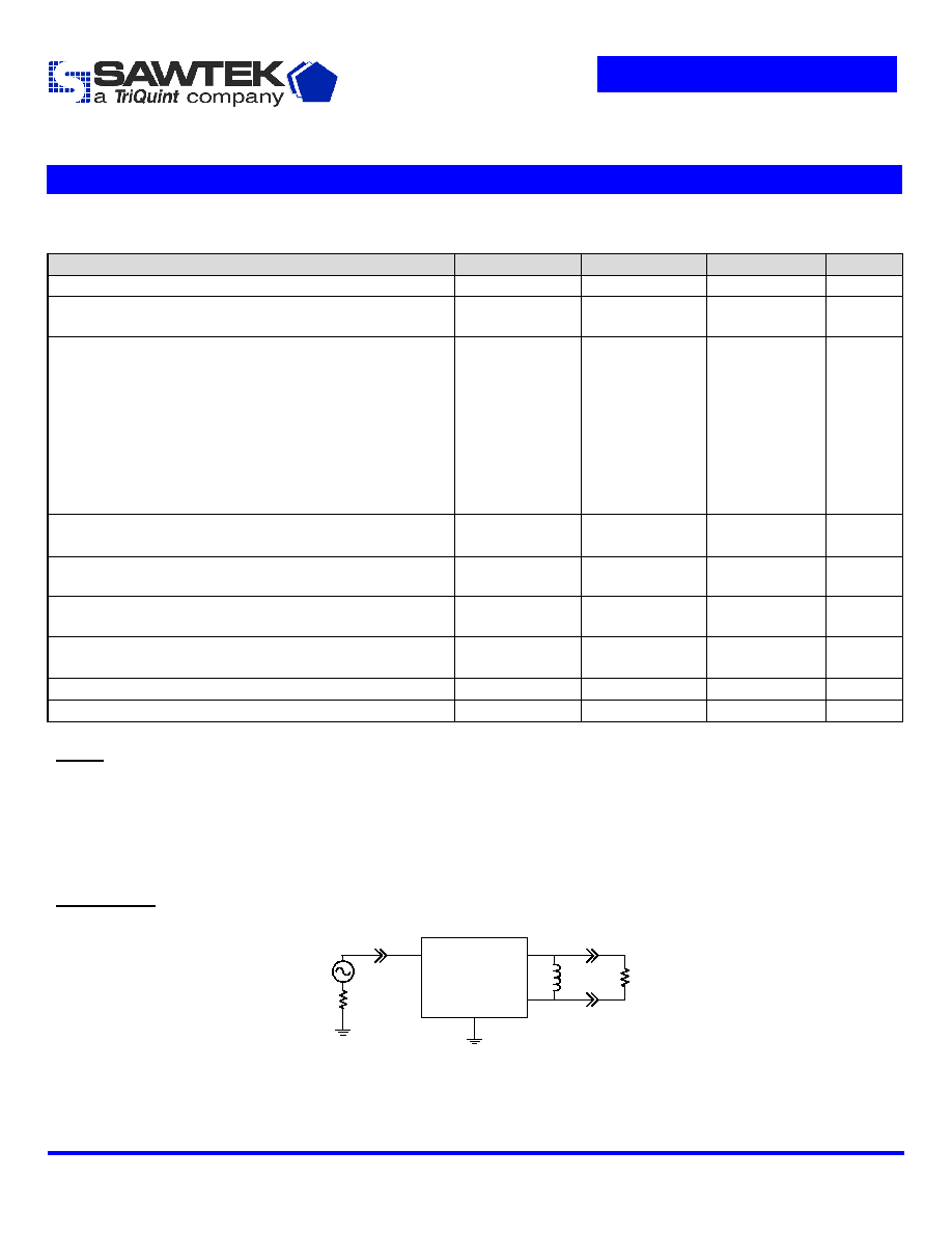
1. All specifications are based on the test circuit shown below
2. This specification is valid for room temperature only. The specification over the full temperature range(s) is available on the next
page(s)
3. Electrical margin has been built into the design to account for the variations due to manufacturing tolerances
4. This is the maximum peak to adjacent valley amplitude change in passband
5. This is the optimum impedance for maximum power transfer
Test Circuit:
Actual matching values may vary due to PCB layout and parasitics
50
Single-ended
Input
2,5
1
3
50
4
200
18nH
200
Balanced
Output

Data Sheet
Part Number 856079
1842.5 MHz SAW Filter
Subject to change or obsolescence without notice
Rev D
05-Sep-2002
Page 3 of 7
Electrical Specifications
(1)
Operating Temperature Range:
(2)
-30 to +80
o
C
Parameter
(3)
Minimum
Typical
Maximum
Unit
Center Frequency
- 1842.5 -
MHz
Maximum Insertion Loss
1805 - 1880 MHz
1805 - 1880 MHz (+15 to
+35
o
C)
-
-
2.8
2.5
3.5
-
dB
dB
Absolute Attenuation
DC - 1000 MHz
1000 - 1710 MHz
1710
-
1765
MHz
1765
-
1785
MHz
1920 - 1980 MHz
1980 - 2090 MHz
2090
-
3000
MHz
3000
-
6000
MHz
40
30
20
8
15
20
30
40
45
34
25
10
17
27
40
50
-
-
-
-
-
-
-
-
dB
dB
dB
dB
dB
dB
dB
dB
Passband Ripple
(4)
1805
-
1880
MHz
-
0.7
1.0
dB
Input/Output Return Loss
1805
-
1880
MHz
8
10
-
dB
Output Amplitude Balance (|S
31
/S
21
|)
1805
-
1880
MHz
-
1.4
2
dB
Output Phase Balance
(S
31
)-
(S
21
)
1805
-
1880
MHz
165
180
190
degree
Source Impedance
- 50 -
Optimal Load Impedance (balanced)
(5)
-
200 || 18nH
-
Notes:
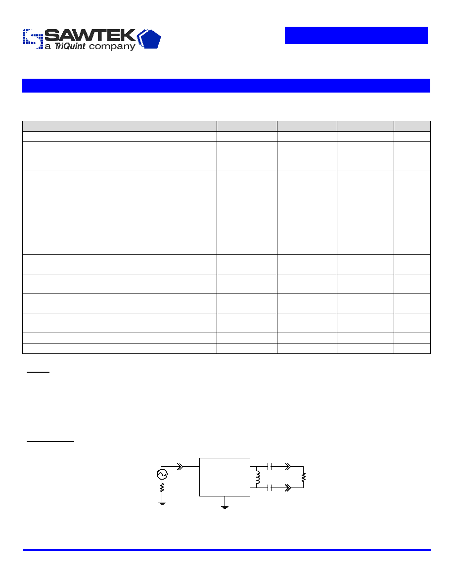
1. All specifications are based on the test circuit shown below
2. In production, devices will be tested at room temperature to a guardbanded specification to ensure electrical compliance over
temperature
3. Electrical margin has been built into the design to account for the variations due to temperature drift and manufacturing tolerances
4. This is the maximum peak to adjacent valley amplitude change in passband
5. This is the optimum impedance for maximum power transfer
Test Circuit:
Actual matching values may vary due to PCB layout and parasitics
50
Single-ended
Input
2,5
1
3
50
4
200
18nH
200
Balanced
Output
Data Sheet
Part Number 856079
1842.5 MHz SAW Filter
Subject to change or obsolescence without notice
Rev D
05-Sep-2002
Page 4 of 7
Electrical Specifications
(1)
Operating Temperature Range:
(2)
-30 to +80
o
C
Parameter
(3)
Minimum
Typical
Maximum
Unit
Center Frequency
- 1842.5 -
MHz
Maximum Insertion Loss
1805 - 1880 MHz
1805 - 1880 MHz (+15 to
+35
o
C)
-
-
3.05
2.75
3.75
-
dB
dB
Absolute Attenuation
DC - 1000 MHz
1000 - 1710 MHz
1710
-
1765
MHz
1765
-
1785
MHz
1920 - 1980 MHz
1980 - 2090 MHz
2090
-
3000
MHz
3000
-
6000
MHz
40
30
20
8
15
20
30
40
45
34
25
10
17
27
40
50
-
-
-
-
-
-
-
-
dB
dB
dB
dB
dB
dB
dB
dB
Passband Ripple
(4)
1805
-
1880
MHz
-
0.7
1.0
dB
Input/Output Return Loss
1805
-
1880
MHz
8
10
-
dB
Output Amplitude Balance (|S
31
/S
21
|)
1805
-
1880
MHz
-
1.4
2
dB
Output Phase Balance
(S
31
)-
(S
21
)
1805
-
1880
MHz
165
180
190
degree
Source Impedance
- 50 -
Optimal Load Impedance (balanced)
(4)
-
200 || 18nH
-
Notes:
1. All specifications are based on the test circuit shown below
2. In production, devices will be tested at room temperature to a guardbanded specification to ensure electrical compliance over
temperature
3. Electrical margin has been built into the design to account for the variations due to temperature drift and manufacturing tolerances
4. This is the maximum peak to adjacent valley amplitude change in passband
5. This is the optimum impedance for maximum power transfer
Test Circuit:
Actual matching values may vary due to PCB layout and parasitics
50
Single-ended
Input
2,5
1
3
50
4
100
6.8nH
1.5pF
1.5pF
100
Balanced
Output
Data Sheet
Part Number 856079
1842.5 MHz SAW Filter
Subject to change or obsolescence without notice
Rev D
05-Sep-2002
Page 5 of 7
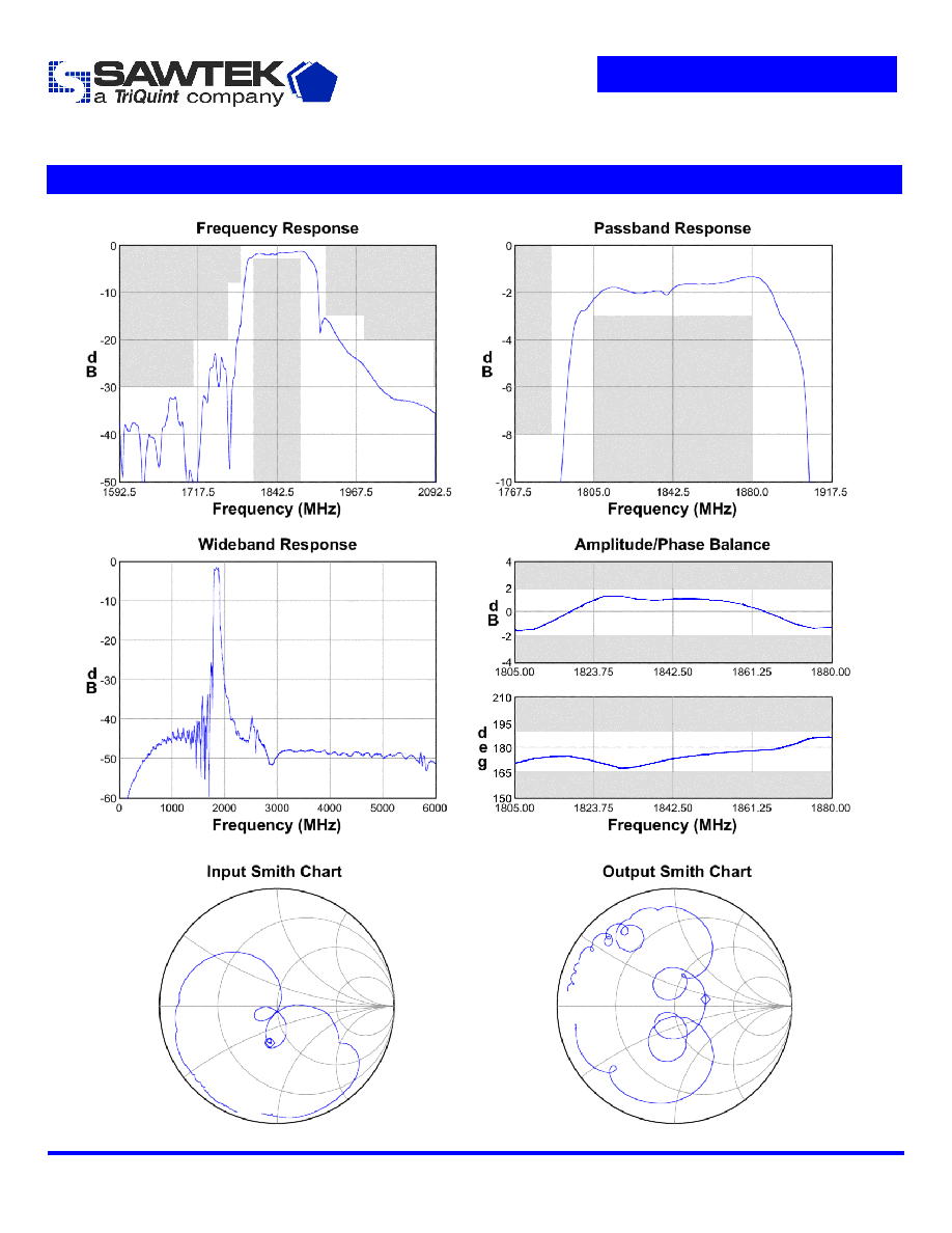
Typical Performance
(at +25
o
C)

Data Sheet
Part Number 856079
1842.5 MHz SAW Filter
Subject to change or obsolescence without notice
Rev D
05-Sep-2002
Page 6 of 7
Matching Schematics
Actual matching values may vary due to PCB layout and parasitics
50
Single-ended
Input
2,5
1
3
50
4
200
18nH
200
Balanced
Output
50
Single-ended
Input
2,5
1
3
50
4
100
6.8nH
1.5pF
1.5pF
100
Balanced
Output
Marking
PCB Footprint
H
JJJYM
ID dot
Date code
Marking
code
logo
Sawtek
.71 SQ
.69
.23
2.08
2.59
The date code consists of: JJJ = Julian day,
Y = last digit of year, M = manufacturing site code
This footprint represents a recommendation only
Dimensions shown are nominal in millimeters
Tape and Reel
1.75
3.5 8.0
A
A
2.0
4.0
4.0
ÿ1.0
ÿ1.5
2.75
1.1
0.254
Section A-A
2.23
2.7
8.8
ÿ330
ÿ102
ÿ20.2
ÿ13.0
2.0
ID dot
Direction of travel
Sawtek
logo
Dimensions shown are nominal in millimeters
Packaging quantity: 10000 units/reel
Data Sheet
Part Number 856079
1842.5 MHz SAW Filter
Subject to change or obsolescence without notice
Rev D
05-Sep-2002
Page 7 of 7
Maximum Ratings
Parameter
Symbol
Minimum
Maximum
Unit
Operating Temperature Range
T
-30
+80
o
C
Storage Temperature Range
T
stg
-40 +85
o
C
Warnings
∑ Electrostatic Sensitive Device (ESD)
∑ Avoid ultrasonic exposure
Links to Additional Technical Information
PCB Layout Tips
Qualification Flowchart
Soldering Profile
S-Parameters
Other Technical Information
Sawtek's liability is limited only to the Surface Acoustic Wave (SAW) component(s) described in this data sheet. Sawtek does not accept any liability for
applications, processes, circuits or assemblies which are implemented using any Sawtek component described in this data sheet.
Contact Information
PO Box 609501
Orlando, FL 32860-9501
USA
Phone: +1 (407) 886-8860
Fax: +1 (407) 886-7061
Email:
custservice@sawtek.com
Web:
www.sawtek.com
Or contact one of our worldwide
Network of
sales offices,
Representatives or distributors