 | –≠–ª–µ–∫—Ç—Ä–æ–Ω–Ω—ã–π –∫–æ–º–ø–æ–Ω–µ–Ω—Ç: 856104 | –°–∫–∞—á–∞—Ç—å:  PDF PDF  ZIP ZIP |
Preliminary Data Sheet
Part Number 856104
1960 MHz SAW Filter
Subject to change or obsolescence without notice
Rev A
10-Sep-2002
Page 1 of 6
Features
∑ For GSM applications
∑ Usable bandwidth 60 MHz
∑ High attenuation
∑ Superior amplitude and phase balance
∑ Single-ended input
∑ Balanced output
∑ Ceramic Surface Mount Package (SMP)
∑ Small size
∑
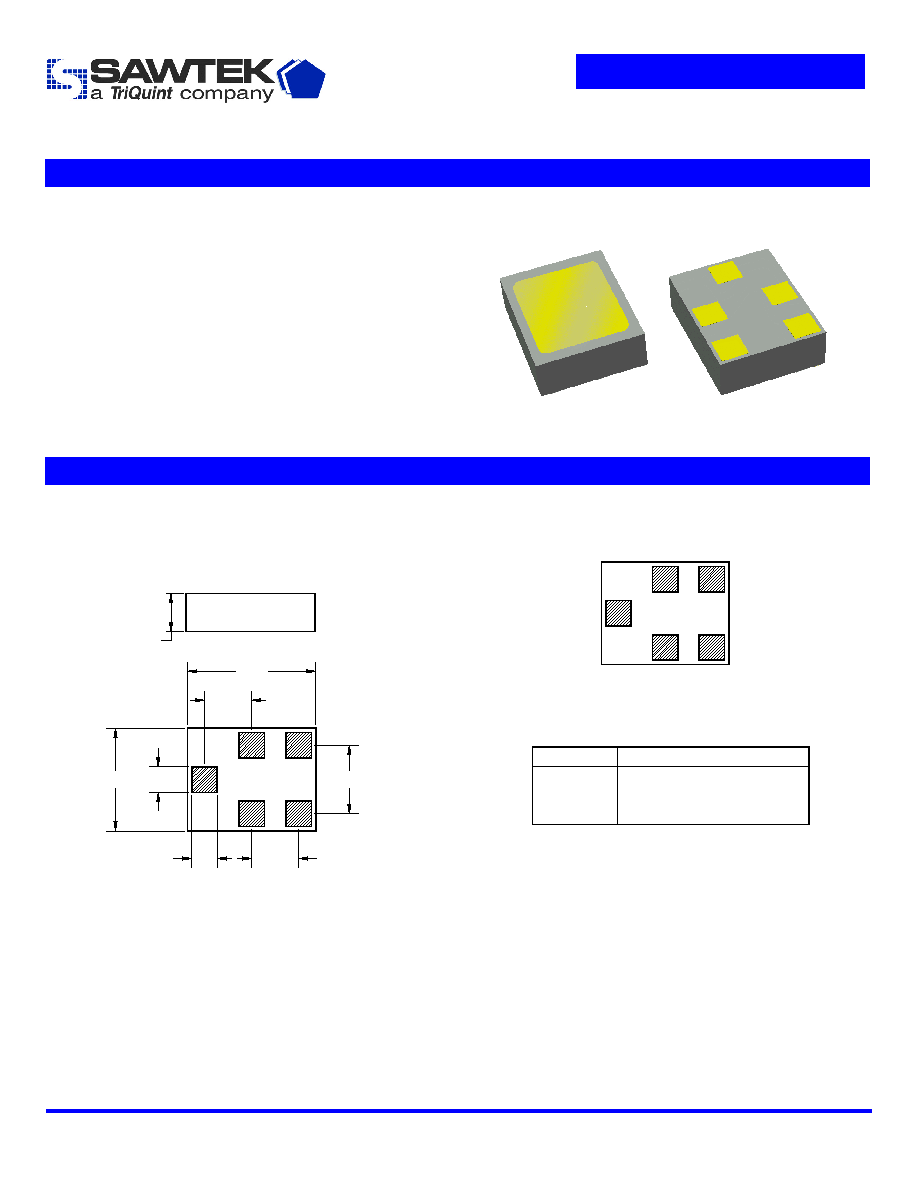
Package
Pin Configuration
Surface Mount 2.50 x 2.00 x 0.76 mm
Bottom View
5
4
3
2
1
Pin No. Description
1
Input,
Unbalanced
2,5
Input, Case ground
3,4
Output,
Balanced
0.76 NOM.
0.84 MAX.
0.50
0.50
2.00
2.50
0.94
1.38
0.94
Dimensions shown are nominal in millimeters
All tolerances are
±0.10mm
Body: Al
2
O
3
ceramic
Lid: Kovar or Alloy 42, Au over Ni plated
Terminations: Au plating 0.5 - 1.0
µm,
over a 2 - 6
µm Ni plating
Preliminary Data Sheet
Part Number 856104
1960 MHz SAW Filter
Subject to change or obsolescence without notice
Rev A
10-Sep-2002
Page 2 of 6
Electrical Specifications
(1)
Operating Temperature Range:
(2)
+25
o
C
Parameter
(3)
Minimum
Typical
Maximum
Unit
Center Frequency
- 1960 -
MHz
Maximum Insertion Loss
1930
-
1990
MHz
-
2.6
3.0
dB
Absolute Attenuation
0
-
1000
MHz
1000
-
1830
MHz
1830
-
1910
MHz
2010
-
2070
MHz
2070
-
3000
MHz
3000
-
5000
MHz
5000
-
6000
MHz
45
28
14
13
22
35
30
55
31
17
15
24
37
34
-
-
-
-
-
-
-
dB
dB
dB
dB
dB
dB
dB
Input/Output Return Loss
1930
-
1990
MHz
8.5
10.5
-
dB
Output Amplitude Balance (|S
31
/S
21
|)
1930
-
1990
MHz
-1.5
0.7
1.5
dB
Output Phase Balance
(S
31
)-
(S
21
)
1930
-
1990
MHz
168
178 -187
192
degree
Source Impedance
- 50 -
Optimal Load Impedance
(4)
-
200 || 16nH
-
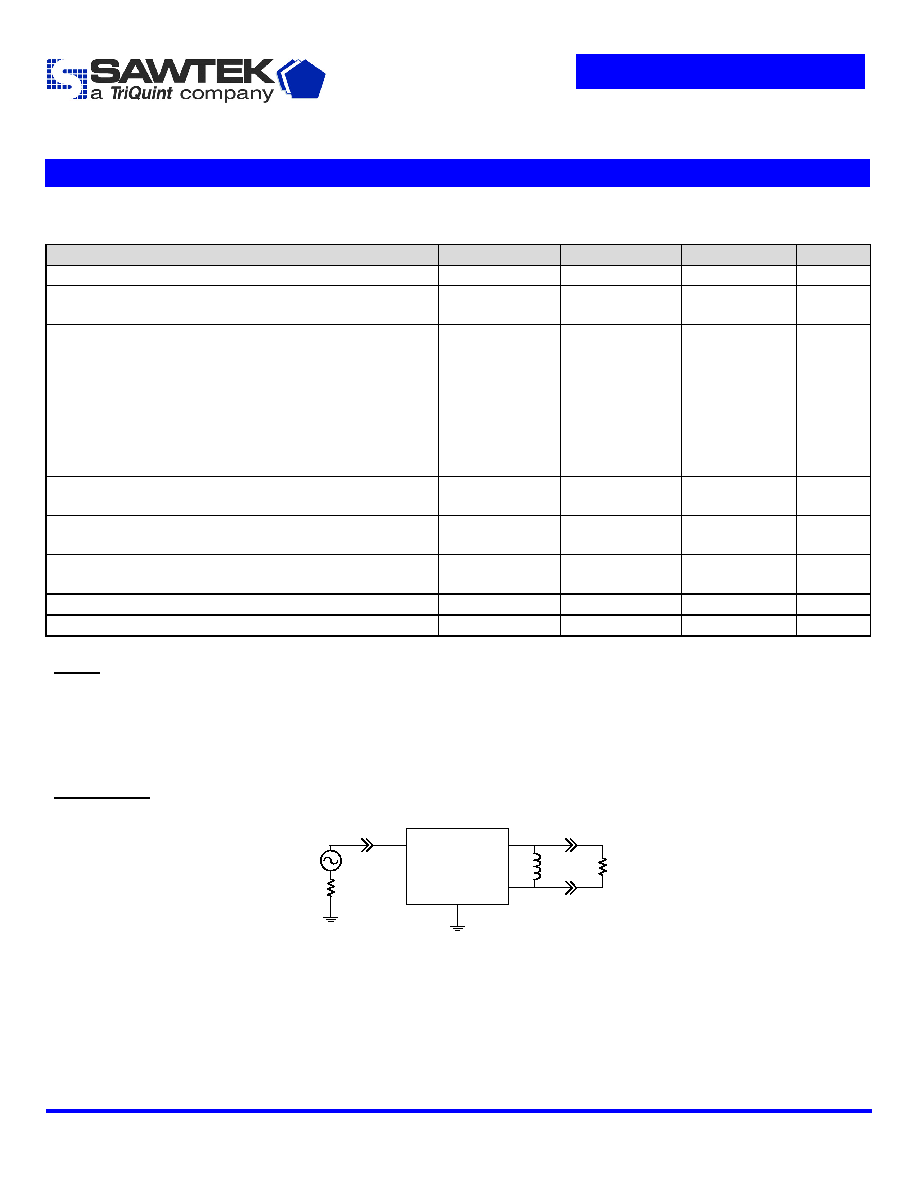
Notes:
1. All specifications are based on the test circuit shown below
2. This specification is valid for room temperature only. The specification over the full temperature range(s) is available on the next
page(s)
3. Electrical margin has been built into the design to account for the variations due to manufacturing tolerances
4. This is the optimum impedance for maximum power transfer given a 50 ohm source impedance
Test Circuit:
Actual matching values may vary due to PCB layout and parasitics
50
Single-ended
Input
2,5
1
3
50
4
200
16nH
200
Balanced
Output

Preliminary Data Sheet
Part Number 856104
1960 MHz SAW Filter
Subject to change or obsolescence without notice
Rev A
10-Sep-2002
Page 3 of 6
Electrical Specifications
(1)
Operating Temperature Range:
(2)
-25 to +80
o
C
Parameter
(3)
Minimum
Typical
Maximum
Unit
Center Frequency
- 1960 -
MHz
Maximum Insertion Loss
1930
-
1990
MHz
1930 - 1990 MHz ( -10 to +75
o
C )
-
-
2.6
2.6
4.0
3.5
dB
dB
Absolute Attenuation
0
-
1000
MHz
1000
-
1830
MHz
1830
-
1910
MHz
2010
-
2070
MHz
2070
-
3000
MHz
3000
-
5000
MHz
5000
-
6000
MHz
45
25
10
7
20
33
30
55
31
17
15
24
37
34
-
-
-
-
-
-
-
dB
dB
dB
dB
dB
dB
dB
Input/Output Return Loss
1930
-
1990
MHz
8.5
10.5
-
dB
Output Amplitude Balance (|S
31
/S
21
|)
1930
-
1990
MHz
-1.5
0.7
1.5
dB
Output Phase Balance
(S
31
)-
(S
21
)
1930
-
1990
MHz
168
178 -187
192
degree
Source Impedance
- 50 -
Optimal Load Impedance
(4)
-
200 || 16nH
-
Notes:
1. All specifications are based on the test circuit shown below
2. In production, devices will be tested at room temperature to a guardbanded specification to ensure electrical compliance over
temperature
3. Electrical margin has been built into the design to account for the variations due to temperature drift and manufacturing tolerances
4. This is the optimum impedance for maximum power transfer given a 50 ohm source impedance
Test Circuit:
Actual matching values may vary due to PCB layout and parasitics
50
Single-ended
Input
2,5
1
3
50
4
200
16nH
200
Balanced
Output

Preliminary Data Sheet
Part Number 856104
1960 MHz SAW Filter
Subject to change or obsolescence without notice
Rev A
10-Sep-2002
Page 4 of 6
Typical Performance
(at +25
o
C)
Preliminary Data Sheet
Part Number 856104
1960 MHz SAW Filter
Subject to change or obsolescence without notice
Rev A
10-Sep-2002
Page 5 of 6
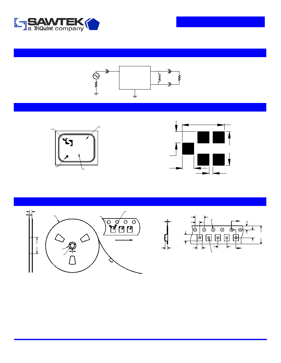
Matching Schematics
Actual matching values may vary due to PCB layout and parasitics
50
Single-ended
Input
2,5
1
3
50
4
200
16nH
200
Balanced
Output
Marking
PCB Footprint
X
JJJYM
ID dot
Date code
Marking
code
logo
Sawtek
.71 SQ
.69
.23
2.08
2.59
The date code consists of: JJJ = Julian day,
Y = last digit of year, M = manufacturing site code
This footprint represents a recommendation only
Dimensions shown are nominal in millimeters
Tape and Reel
1.75
3.5 8.0
A
A
2.0
4.0
4.0
ÿ1.0
ÿ1.5
2.75
1.1
0.254
Section A-A
2.23
2.7
8.8
ÿ330
ÿ102
ÿ20.2
ÿ13.0
2.0
ID dot
Direction of travel
Sawtek
logo
Dimensions shown are nominal in millimeters
Packaging quantity: 10000 units/reel