 | –≠–ª–µ–∫—Ç—Ä–æ–Ω–Ω—ã–π –∫–æ–º–ø–æ–Ω–µ–Ω—Ç: 856234 | –°–∫–∞—á–∞—Ç—å:  PDF PDF  ZIP ZIP |
Data Sheet
Part Number 856234
183.6 MHz SAW Filter
Features
∑ For CDMA handset IF applications
∑ Usable bandwidth of 1.26 MHz
∑ Low loss
∑ High attenuation at tones
∑ Single-ended or balanced operation
∑ Ceramic Surface Mount Package (SMP)
∑ Small size
∑
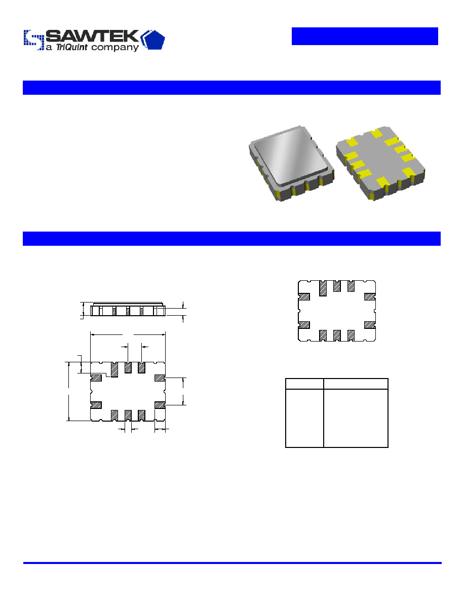
Package
Pin Configuration
Surface Mount 7.00 x 5.50 x 1.24 mm
Bottom View
9
10
7
8
6
4
5
1
2
3
Pin No. Description
4
Output
5
Output
return
9
Input
10
Input
return
1,2,3
6,7,8
Case ground
Case ground
5.50
0.60
1.24 NOM.
1.35 MAX.
1.40
2.54
1.00
7.00
1.27
0.69
Dimensions shown are nominal in millimeters
All tolerances are
±0.15mm except overall
length and width
±0.13mm
Body: Al
2
O
3
ceramic
Lid: Kovar, Ni plated
Terminations: Au plating 0.5 - 1.0
µm,
over a 2 - 6
µm Ni plating
Subject to change or obsolescence without notice
Rev B
04-Mar-2003
Page 1 of 5
Data Sheet
Part Number 856234
183.6 MHz SAW Filter
Subject to change or obsolescence without notice
Rev B
04-Mar-2003
Page 2 of 5
Electrical Specifications
(1)
Operating Temperature Range:
(2)
-30 to +85
o
C
Parameter
(3)
Minimum
Typical
Maximum
Unit
Center Frequency, f
0
- 183.6 -
MHz
Insertion Loss at 183.6 MHz
Excluding losses due to matching
Including losses in matching test circuit shown below
-
-
7.4
9.8
9.2
11.6
dB
dB
Lower 5 dB Point
Upper 5 dB Point
-
184.230
182.893
184.311
182.970
-
MHz
MHz
Amplitude Variation
183.3 - 183.9 MHz
-
0.4
1.25
dB p-p
RMS Phase Variation
182.97 - 184.23 MHz
-
1.6
3.2
deg RMS
Attenuation
(4)
f
0
- 2.05 MHz
f
0
- 1.70 MHz
f
0
- 1.25 MHz
f
0
- 0.90 MHz
f
0
+ 0.90 MHz
f
0
+ 1.25 MHz
f
0
+ 1.70 MHz
f
0
+ 2.05 MHz
33
33
33
33
33
33
33
33
45
40
40
38
40
36
40
40
-
-
-
-
-
-
-
-
dB
dB
dB
dB
dB
dB
dB
dB
Rejection
(4)
10.0
-
171.6
MHz
171.6
-
174.6
MHz
174.6
-
182.7
MHz
184.5
-
192.6
MHz
192.6
-
195.6
MHz
195.6
-
367.2
MHz
45
38
33
33
38
45
60
50
38
36
48
50
-
-
-
-
-
-
dB
dB
dB
dB
dB
dB
Optimal Source Impedance
(5)
-
800
||49nH
-
Optimal Load Impedance
(5)
-
380
||39.5nH
-
Notes:
1. All specifications are based on the test circuit shown below
2. In production, devices will be tested at room temperature to a guardbanded specification to ensure electrical compliance over
temperature
3. Electrical margin has been built into the design to account for the variations due to manufacturing tolerances
4. Relative to insertion loss at 183.6 MHz
5. This is the complex conjugate of the unmatched filter's impedance resulting in maximum power transfer
Test Circuit:
Actual matching values may vary due to PCB layout and parasitics
1000
Single-ended
input
1000
47pF
47nH
120pF
120pF
43nH
500
0.5pF
9
5
4
1,2,3
6,7,8,10
500
Balanced
output
Data Sheet
Part Number 856234
183.6 MHz SAW Filter
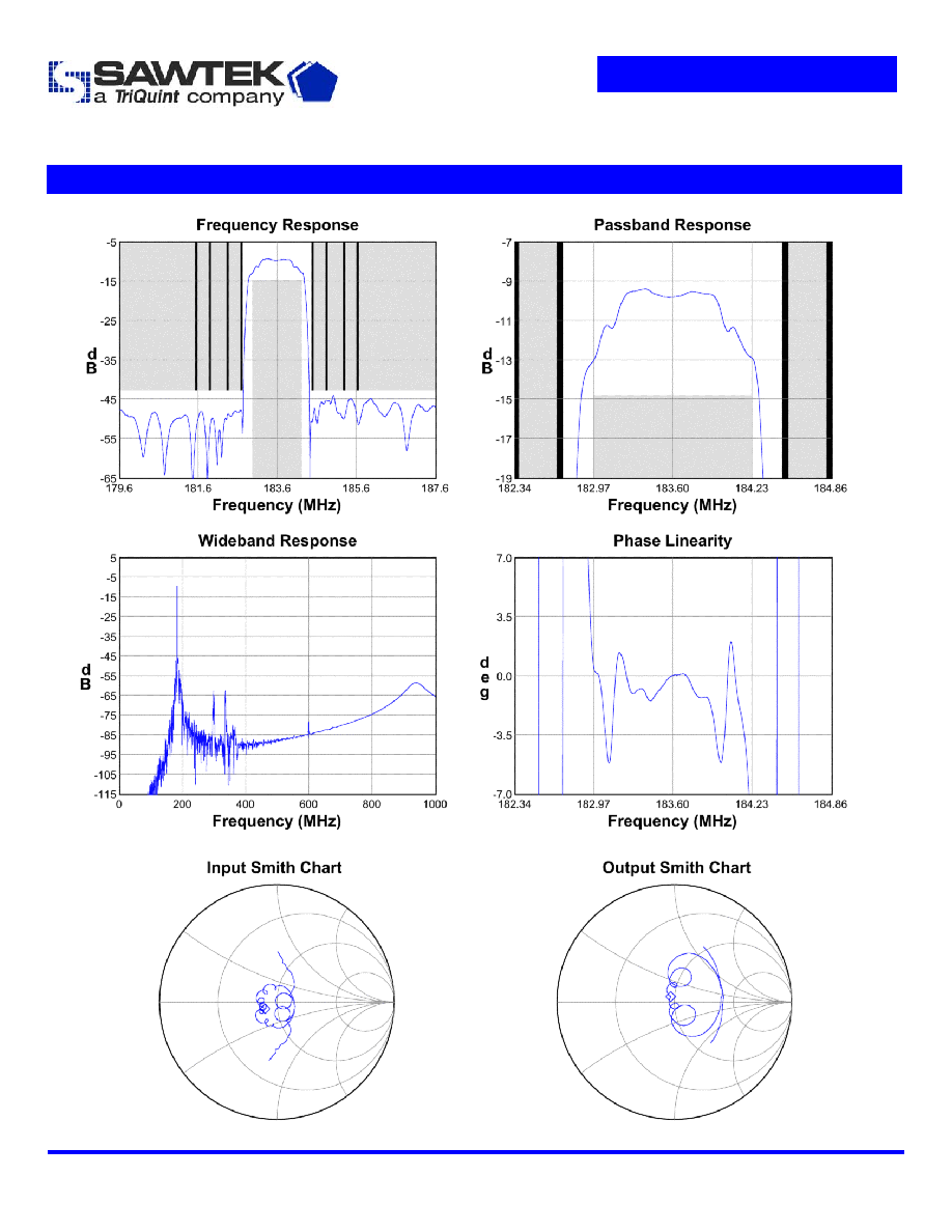
Typical Performance
(at +25
o
C)
Subject to change or obsolescence without notice
Rev B
04-Mar-2003
Page 3 of 5
Data Sheet
Part Number 856234
183.6 MHz SAW Filter
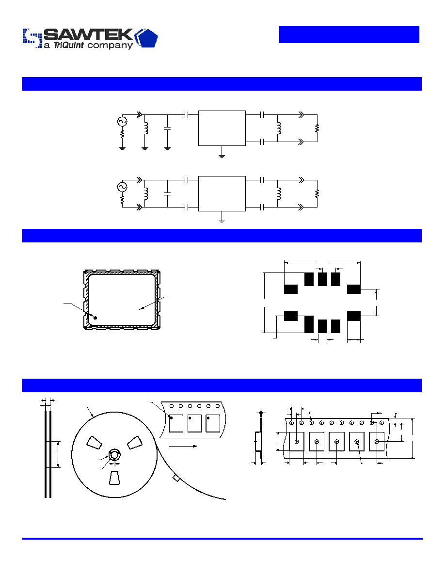
Matching Schematics
Actual matching values may vary due to PCB layout and parasitics
1000
Single-ended
input
1000
47pF
47nH
120pF
120pF
43nH
500
0.5pF
9
5
4
1,2,3
6,7,8,10
500
Balanced
output
1000
Balanced
input
1000
68pF
56nH
68pF
120pF
120pF
43nH
500
0.5pF
10
9
5
4
1,2,3
6,7,8
500
Balanced
output
Marking
PCB Footprint
Date code
856234
SAWTEK
ID dot
XXXXXX
0.80
1.60
5.70
1.27
1.20
2.54
7.20
The date code consists of: day of the current year (Julian,
3 digits), last digit of the year (1 digit) and hour (2 digits)
This footprint represents a recommendation only
Dimensions shown are nominal in millimeters
Tape and Reel
Section A-A
0.3
2.2
7.3
5.8
ÿ1.5
8.0
4.0
2.0
A
A
ÿ1.5
16.0
7.5
1.75
Pad 1 ID dot
2.0
ÿ13.0
ÿ20.2
ÿ330
16.8
2.7
Direction of travel
ÿ102
Dimensions shown are nominal in millimeters
Packaging quantity: 3000 units/reel
Subject to change or obsolescence without notice
Rev B
04-Mar-2003
Page 4 of 5
Data Sheet
Part Number 856234
183.6 MHz SAW Filter
Maximum Ratings
Parameter
Symbol
Minimum
Maximum
Unit
Operating Temperature Range
T
-30
+85
o
C
Storage Temperature Range
T
stg
-40 +85
o
C
Warnings
∑ Electrostatic Sensitive Device (ESD)
∑ Avoid ultrasonic exposure
Links to Additional Technical Information
PCB Layout Tips
Qualification Flowchart
S-Parameters
Sawtek's liability is limited only to the Surface Acoustic Wave (SAW) component(s) described in this data sheet. Sawtek does not accept any liability for
applications, processes, circuits or assemblies which are implemented using any Sawtek component described in this data sheet.
Contact Information
PO Box 609501
Orlando, FL 32860-9501
USA
Phone: +1 (407) 886-8860
Fax: +1 (407) 886-7061
Email:
custservice@sawtek.com
Web:
www.sawtek.com
Or contact one of our worldwide
network of
sales offices,
representatives or distributors
Soldering Profile
Other Technical Information
Subject to change or obsolescence without notice
Rev B
04-Mar-2003
Page 5 of 5