 | –≠–ª–µ–∫—Ç—Ä–æ–Ω–Ω—ã–π –∫–æ–º–ø–æ–Ω–µ–Ω—Ç: 856308 | –°–∫–∞—á–∞—Ç—å:  PDF PDF  ZIP ZIP |
Preliminary Data Sheet
Part Number 856308
1575.42 MHz SAW Filter
Subject to change or obsolescence without notice
Rev -
16-Dec-2002
Page 1 of 5
Features
∑
For GPS applications
∑
Usable bandwidth 2 MHz
∑
Very Low loss
∑
Single-ended operation at 50
∑
No impedance matching required for operation
at 50
∑
Single-ended operation
∑
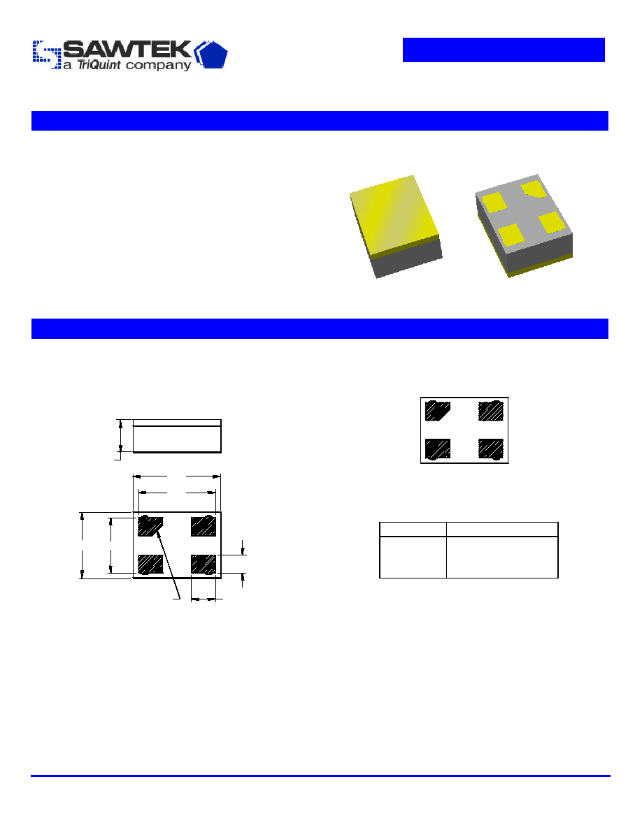
Chip Scale Package (CSP)
∑
Ceramic surface mount package
∑
Hermetic
∑
Package
Pin Configuration
Surface Mount 2.00 x 1.50 x 0.76 mm
Bottom View
3
4
2
1
Pin No.
Description
1
Input
3
Output
2,4
Case ground
0.76 NOM.
0.84 MAX.
1.30
1.50
0.42
0.56
0.25x45∞ CHAMFER
1.80
2.00
Dimensions shown are nominal in millimeters
All tolerances are
±
0.10mm
Body: Al
2
O
3
ceramic
Lid: Kovar or Alloy 42, Au over Ni plated
Terminations: Au plating 0.5 - 1.0
µ
m,
over a 2 - 6
µ
m Ni plating
Preliminary Data Sheet
Part Number 856308
1575.42 MHz SAW Filter
Subject to change or obsolescence without notice
Rev -
16-Dec-2002
Page 2 of 5
Electrical Specifications
(1)
Operating Temperature Range:
(2)
-40 to +85
o
C
Parameter
(3)
Minimum
Typical
Maximum
Unit
Center Frequency
-
1575.42
-
MHz
Insertion Loss
1574.42 - 1576.42 MHz
-
1.0
1.4
dB
Absolute Attenuation
0 - 1475 MHz
1475 - 1522.42 MHz
1628.42 - 1750 MHz
1750 - 1800 MHz
1800 - 1990 MHz
1990 - 3000 MHz
3000 - 4000 MHz
4000 - 6000 MHz
30
30
30
32
32
30
20
17
36
33
37
36
38
40
25
22
-
-
-
-
-
-
-
-
dB
dB
dB
dB
dB
dB
dB
dB
Passband Variation
1574.42 - 1576.42 MHz
-
0.25
0.5
dB p-p
Input/Output Return Loss
1574.42 - 1576.42 MHz
10
18
-
dB
Source Impedance
(4)
-
50
-
Load Impedance
(4)
-
50
-
Notes:
1. All specifications are based on the test circuit shown below
2. In production, devices will be tested at room temperature to a guardbanded specification to ensure electrical compliance over
temperature
3. Electrical margin has been built into the design to account for the variations due to temperature drift and manufacturing tolerances
4. This is the optimum impedance in order to achieve the performance shown
Test Circuit:
50
Single-ended
2,4
1
3
50
50
No impedance matching
required
Preliminary Data Sheet
Part Number 856308
1575.42 MHz SAW Filter
Subject to change or obsolescence without notice
Rev -
16-Dec-2002
Page 3 of 5
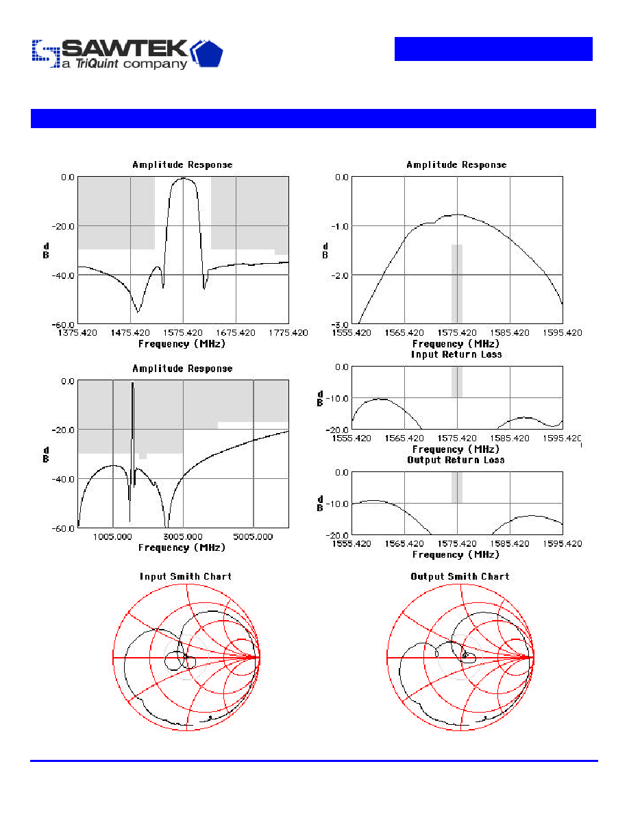
Typical Performance
(at +25
o
C)
Preliminary Data Sheet
Part Number 856308
1575.42 MHz SAW Filter
Subject to change or obsolescence without notice
Rev -
16-Dec-2002
Page 4 of 5
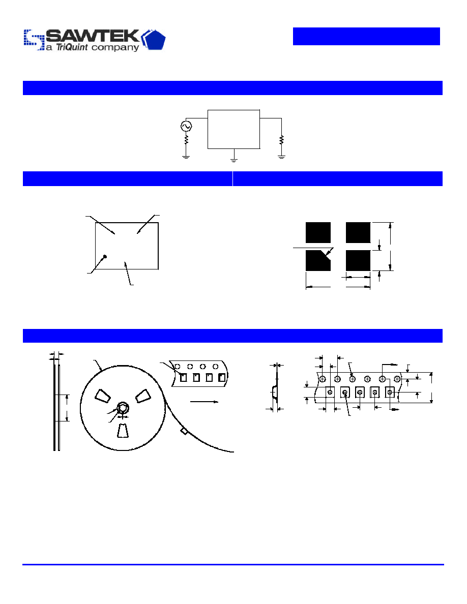
Matching Schematics
50
Single-ended
2,4
1
3
50
50
No impedance matching
required
Marking
PCB Footprint
Marking
code
MFG site
X M
X X Y
ID dot
Date code
0.31x45∞
CHAMFER
0.76
2.00
0.62
1.50
The date code consists of: JJJ = Julian day,
Y = last digit of year, M = manufacturing site code
This footprint represents a recommendation only
Dimensions shown are nominal in millimeters
Tape and Reel
1.83
Section A-A
0.3
1.09
2.34
ÿ1.5
ÿ1.0
4.0
4.0
2.0
A
A
8.0
3.5
1.75
8.8
ID dot
2.0
Direction of travel
ÿ330
ÿ20.2
ÿ13.0
ÿ102
2.7
Dimensions shown are nominal in millimeters
Packaging quantity: 10000 units/reel
Preliminary Data Sheet
Part Number 856308
1575.42 MHz SAW Filter
Subject to change or obsolescence without notice
Rev -
16-Dec-2002
Page 5 of 5
Maximum Ratings
Parameter
Symbol
Minimum
Maximum
Unit
Operating Temperature Range
T
-30
+85
o
C
Storage Temperature Range
T
stg
-40
+85
o
C
Warnings
∑
Electrostatic Sensitive Device (ESD)
∑
Avoid ultrasonic exposure
Links to Additional Technical Information
PCB Layout Tips
Qualification Flowchart
Soldering Profile
S-Parameters
Other Technical Information
Sawtek's liability is limited only to the Surface Acoustic Wave (SAW) component(s) described in this data sheet. Sawtek does not accept any liability for
applications, processes, circuits or assemblies which are implemented using any Sawtek component described in this data sheet.
Contact Information
PO Box 609501
Orlando, FL 32860-9501
USA
Phone: +1 (407) 886-8860
Fax: +1 (407) 886-7061
Email:
custservice@sawtek.com
Web:
www.sawtek.com
Or contact one of our worldwide
Network of
sales offices,
Representatives or distributors