 | –≠–ª–µ–∫—Ç—Ä–æ–Ω–Ω—ã–π –∫–æ–º–ø–æ–Ω–µ–Ω—Ç: CGB240 | –°–∫–∞—á–∞—Ç—å:  PDF PDF  ZIP ZIP |

CGB 240
Datasheet
Description:
The CGB240 GaAs Power Amplifier MMIC has been
especially developed for wireless applications in the
2.4 - 2.5 GHz ISM band (e.g. Bluetooth class 1). Its
high power added efficiency and single positive sup-
ply operation makes the device ideally suited to
handheld applications. The device delivers 23 dBm
output power at a supply voltage of 3.2 V, with an
overall
PAE
of 50%. The output power can be ad-
justed using an analog control voltage (
V
CTR
). Simple
external input-, interstage-, and output matching cir-
cuits are used to adapt to the different requirements
of linearity and harmonic suppression in various ap-
plications.
For WLAN applications (IEEE802.11b) or appli-
cations serving both WLAN and Bluetooth, we
recommend to use the CGB240B device.
Features:
∑
Single voltage supply.
∑
Wide operating voltage range 2.0 - 5.5 V.
∑ P
OUT
= 23 dBm at
V
C
= 3.2 V.
∑
Overall power added efficiency (PAE) typi-
cally 50%.
∑
High
PAE
at low≠power mode.
∑
Analog power control with four power
steps.
∑
Straight-Forward Matching; Few external
components.
Applications:
∑
Bluetooth Class 1
∑
Cordless Phones
∑
Home RF
2-Stage Bluetooth InGaP HBT Power Amplifier
Package Outline:
1
5
TSSOP-10-2
MSOP-10
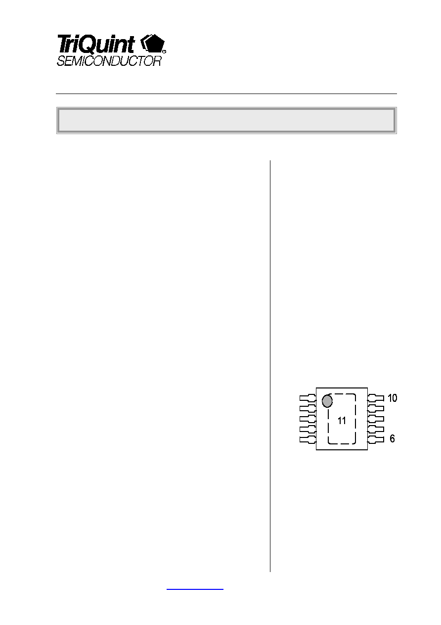
Pin Configuration:
1 & 2:
Vc1
3:
RF In
4, 5, & 10:
NC
6:
Vcntrl1
7:
Vcntrl2
8 & 9:
Vc2
11 (Paddle): GND
For further information please visit
www.triquint.com
pg.
2/13
Rev. 1.6 October 20th, 2004

CGB 240 Datasheet
Absolute Maximum Ratings:
Parameter
Symbol
Min.
Max.
Units
Supply voltage- CW
V
cc
0
5.5
V
dc
Supply voltage- Pulsed
V
cc
0
5.0
V
dc
Power control voltage
V
apc
0
3.2
V
DC supply current- Stage 1
I
cc
0
40.0
mA
DC supply current- Stage 2
I
cc
0
160.0
mA
Total Power Dissipation
1
P
TOT
0.5
W
RF Input Power
2
P
IN, MAX
+10
dBm
RF Output Power
2
P
OUT, MAX
+25
dBm
Operating case temperature
T
a
-20
85
∫C
Storage temperature
T
s
-55
150
∫C
1
Thermal resistance between junction and pad 11 ( = heatsink ):
R
THCH
= 100 K/W.
2
No RF input signal should be applied before turn-on of DC Power. An output VSWR of 1:1 is as-
sumed.
Electrical Characteristics of CGB240 Device used in Bluetooth PA Reference
Design (See Application Note 1)
T
A
= 25 ∞C;
V
CC
= 3.2 V;
f
= 2.4 ... 2.5 GHz;
Z
IN
=
Z
OUT
= 50 Ohms
Parameter
Symbol
Limit Values
Unit
Test Conditions
min
typ
max
Supply Current
Small-Signal Operation
I
CC,SS
125
150
mA
P
IN
= - 10 dBm
V
CTR
= 2.5 V
Power Gain
Small-Signal Operation
G
SS
23 26 dB
P
IN
= - 10 dBm
V
CTR
= 2.5 V
Output Power
Power Step 1
P
OUT,1
7
dBm
P
IN
= + 3 dBm
V
CTR
= 1.15 V
Supply Current
Power Step 1
I
CC,1
15
mA
P
IN
= + 3 dBm
V
CTR
= 1.15 V
Power Added Efficiency
Power Step 1
PAE
1
10
%
P
IN
= + 3 dBm
V
CTR
= 1.15 V
For further information please visit
www.triquint.com
pg.
3/13
Rev. 1.6 October 20th, 2004

CGB 240 Datasheet
Electrical Characteristics of CGB240 used in PA Reference Design (cont.)
Parameter
Symbol
Limit Values
Unit
Test Conditions
Min
Typ
Max
Output Power
Power Step 2
P
OUT,2
12
dBm
P
IN
= + 3 dBm
V
CTR
= 1.3 V
Supply Current
Power Step 2
I
CC,2
25
mA
P
IN
= + 3 dBm
V
CTR
= 1.3 V
Power Added Efficiency
Power Step 2
PAE
2
20
%
P
IN
= + 3 dBm
V
CTR
= 1.3 V
Output Power
Power Step 3
P
OUT,3
17
dBm
P
IN
= + 3 dBm
V
CTR
= 1.5 V
Supply Current
Power Step 3
I
CC,3
52
mA
P
IN
= + 3 dBm
V
CTR
= 1.5 V
Power Added Efficiency
Power Step 3
PAE
3
32
%
P
IN
= + 3 dBm
V
CTR
= 1.5 V
Output Power
Power Step 4
P
OUT,4
22 23 24
dBm
P
IN
= + 3 dBm
V
CTR
= 2.5 V
Supply Current
Power Step 4
I
CC,4
125
mA
P
IN
= + 3 dBm
V
CTR
= 2.5 V
Power Added Efficiency
Power Step 4
PAE
4
40 50 - %
P
IN
= + 3 dBm
V
CTR
= 2.5 V
2
nd
Harm. Suppression
Power Step 4
h
2
-
35
dBc
P
IN
= + 3 dBm
V
CTR
= 2.5 V
3
rd
Harm. Suppression
Power Step 4
h
3
-
50
dBc
P
IN
= + 3 dBm
V
CTR
= 2.5 V
Turn-Off Current
I
CC,OFF
1
uA
V
CC
= 3.2 V;
V
CTR
<
0.4 V; No RF Input
Off-State Isolation
S
21,0
26
dB
P
IN
= + 3 dBm
V
CTR
= 0 V
Rise Time 1 )
T
R1
1
µs
V
CC
= 5.0 V
V
CTR
= 0 to 1V Step
Rise Time 2
1)
T
R2
1
µs
V
CC
= 5.0 V
V
CTR
= 0 to 3V Step
Fall Time 1
1)
T
F1
1
µs
V
CC
= 5.0 V
V
CTR
= 1 to 0V Step
Fall Time 2
1)
T
F2
1
µs
V
CC
= 5.0 V
V
CTR
= 3 to 0V Step
Maximum Load VSWR
(no damage to device)
allowed for 10s
VSWR
6
P
IN
= + 5 dBm;
V
CC
=
4.8 V;
V
CTR
= 2.5 V
Z
IN
= 50 Ohms
1) Rise time
T
R:
time between turn-on of
V
CTR
voltage until reach of 90% of full output power level.
Fall time
T
F:
as time between turn-off of
V
CTR
voltage until reach of 10% of full output power level.
Please note: Reduced Vccp,max for pulsed operation applies (see "absolute maximum ratings").
For further information please visit
www.triquint.com
pg.
4/13
Rev. 1.6 October 20th, 2004

CGB 240 Datasheet
S≠Parameters for Linear Small-Signal Operation
T
A
= 25 ∞C;
V
CC
= 2.8 to 3.2 V;
V
CTR
= 2.5 to 2.8 V;
f
= 2.4 ... 2.5 GHz
P
IN
< - 4 dBm; Interstage match pin terminated with (1 + j 12.5) Ohms.
Parameter (Target Data)
Symbol
Typ. Value
Unit
Magnitude Input Reflection
MAG (
S
11
)
0.67
Phase Input Reflection
ANG (
S
11
)
+ 180
Degrees
Magnitude Forward Power Gain
2)
MAG (
S
21
)
20 dB
Magnitude Reverse Power Gain
2
)
MAG (
S
12
)
≠ 47
dB
Magnitude Output Reflection )
MAG (
S
22
)
0.59
Phase Output Reflection
2
)
ANG (
S
22
)
+ 147
Degrees
2
)
Measured for small signal conditions in pure 50 Ohm environment.
For further information please visit
www.triquint.com
pg.
5/13
Rev. 1.6 October 20th, 2004

CGB 240 Datasheet
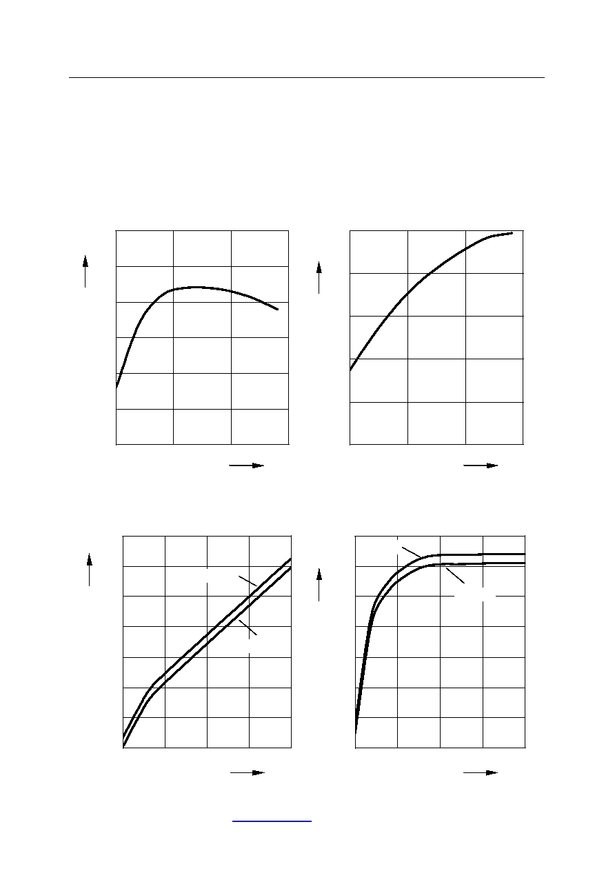
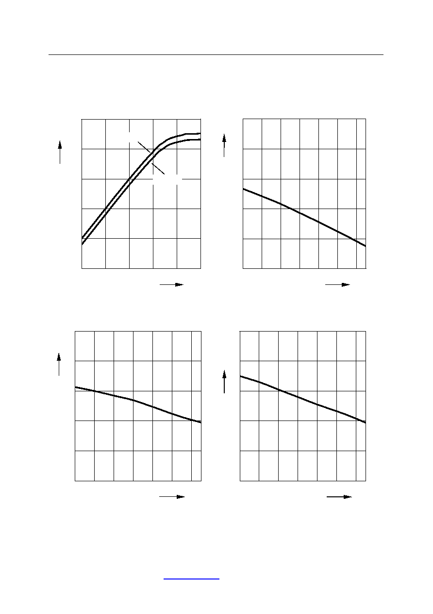
Typical Device Performance for Reference Design (see Application Note 1)
Valid for all plots:
T
A
= 25 ∞C;
V
CC
= 3.2 V;
V
CTR
= 2.5 V;
f
= 2.4 ... 2.5 GHz;
Z
IN
=
Z
OUT
= 50 Ohms. Changes from these values noted.
Efficiency
PAE
=
f
(
V
CC
) Output
Power
P
OUT
=
f
(
V
CC
)
P
IN
= +3dBm
P
IN
= +3dBm
30,0
35,0
40,0
45,0
50,0
55,0
60,0
2,0
3,0
4,0
5,0
Supply Voltage Vcc
Pow
e
r
A
dded E
f
f
i
c
i
enc
y
P
A
E
%
V
15,0
17,0
19,0
21,0
23,0
25,0
2,0
3,0
4,0
5,0
Supply Voltage Vcc
O
u
t
put
P
o
w
e
r
P
out
dBm
V
Supply Current
I
CC
=
f
(
V
CTR
) Output
Power
P
OUT
=
f
(
V
CTR
)
P
IN
= +3dBm
P
IN
= +3dBm
0,0
20,0
40,0
60,0
80,0
100,0
120,0
140,0
1,0
1,5
2,0
2,5
3,0
Vctr
S
upply
C
u
r
r
ent
I
c
c
mA
V
Vcc=3.2V
Vcc=2.8V
-10,0
-5,0
0,0
5,0
10,0
15,0
20,0
25,0
1,0
1,5
2,0
2,5
3,0
Vctr
O
u
t
put
P
o
w
e
r
P
out
dBm
V
Vcc=3.2V
Vcc=2.8V
For further information please visit
www.triquint.com
pg.
6/13
Rev. 1.6 October 20th, 2004

CGB 240 Datasheet
Output Power Compression
P
OUT
=
f
(
P
CIN
) Supply
Current
I
CC
=
f
(
T
A
)
P
IN
= +3dBm
P
IN
= +3dBm, Vcc = 3.2V
0,0
5,0
10,0
15,0
20,0
25,0
-20,0
-15,0
-10,0
-5,0
0,0
5,0
Input Power Pin
O
u
t
put
P
o
w
e
r
P
out
dBm
dBm
Vcc=3.2V
Vcc=2.8V
100
110
120
130
140
150
-40
-20
0
20
40
60
80
Ambient Temperature Ta
Tot
a
l
S
u
ppl
y
Current
I
c
c
mA
Deg C
Output Power
P
OUT
=
f
(
T
A
) Small-Signal
Gain
S
21
=
f
(
T
A
)
P
IN
= +3dBm
P
IN
= -10 dBm, Vcc = 3.2V
20
21
22
23
24
25
-40
-20
0
20
40
60
80
Ambient Temperature Ta
Ou
t
put
P
o
wer P
out
dBm
Deg C
20
22
24
26
28
30
-40
-20
0
20
40
60
80
Ambient Temperature Ta
SS G
a
in
dB
Deg C
For further information please visit
www.triquint.com
pg.
7/13
Rev. 1.6 October 20th, 2004

CGB 240 Datasheet
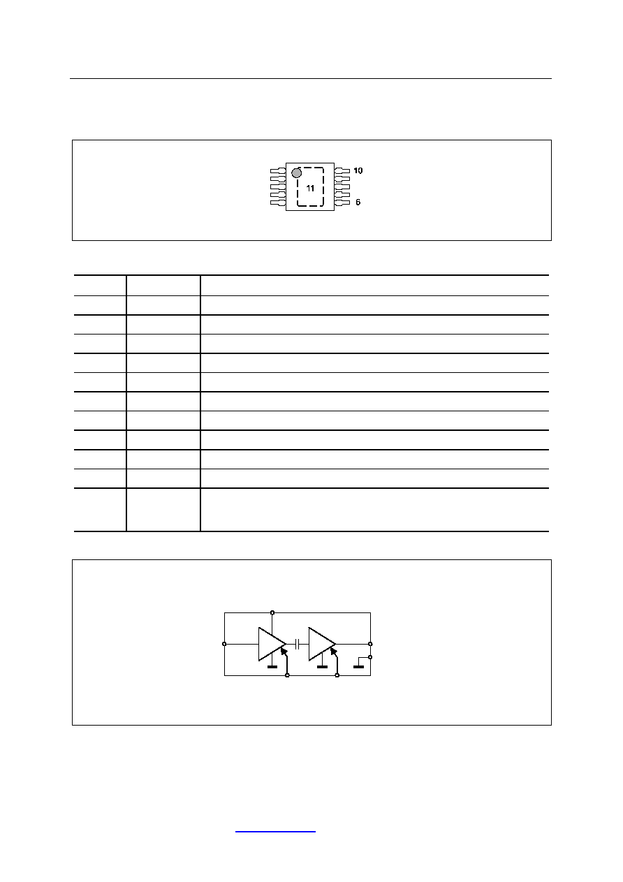
Pinning
1
5
TSSOP-10
MSOP-10
Figure 1
CGB240 Outline
Pad Symbol Function
1 V
C1
Supply voltage of 1
st
stage / interstage match
2 V
C1
Supply voltage of 1
st
stage / interstage match
3 RF
IN
RF input
4 N.C.
5 N.C.
6 V
CTR1
Control voltage 1
st
stage
7 V
CTR2
Control voltage 2
nd
stage
8 V
C2
Supply voltage of 2
nd
stage / RF output
9 V
C2
Supply voltage of 2
nd
stage / RF output
10 N.C.
11 GND
RF and DC ground (pad located on backside of package)
Heatsink. Thermal resistance between junction ≠ pad 11:
R
THCH
= 100
K/W.
Functional Diagram
(3)
RFin
(1,2)
Vc1
(8,9) Vc2
(6)
Vctr1
(7)
Vctr2
(11) Gnd
Figure 2
CGB240 Functional Diagram
For further information please visit
www.triquint.com
pg.
8/13
Rev. 1.6 October 20th, 2004

CGB 240 Datasheet
Application Note 1: Bluetooth CGB240 PA Reference Design (TRL matching)
RF In
RF Out
Vcc
Vctr
C1
C4
C5
TRL1
TRL2
CGB240
L1
TRL3
R1
C7
C6
C3
C2
1
5
6
10
11
Figure 3
Schematic of Bluetooth CGB240 PA reference design.
Part Type
Value
Outline
Source
Part
No.
C1
Cer. Capacitor
22 pF
0402
Murata COG
C2
Cer. Capacitor
22 pF
0402
Murata COG
C3 )
Cer. Capacitor
1.5 pF
0603
AVX ACCU-P
06035J1R5BBT
C4
Cer. Capacitor
2.2 pF
0402
Murata COG
C5
Cer. Capacitor
10 pF
0402
Murata COG
C6
Cer. Capacitor
1 µF
0603
Murata X7R
C7
Cer. Capacitor
1 nF
0402
Murata X7R
L1 Inductor
22
nH
0603 Toko
LL1608≠FS
R1 Resistor
10
R
0402 Mira
TRL1 ) Microstrip
Line
l
= 2,5 mm; FR4 substrate;
h
= 0,2 mm;
w
= 0,32 mm
TRL2
4)
Microstrip
Line
l
= 1,8 mm; FR4 substrate;
h
= 0,2 mm;
w
= 0,32 mm
TRL3
4)
Microstrip
Line
l
= 4,0 mm; FR4 substrate;
h
= 0,2 mm;
w
= 0,32 mm
3
)
Cost optimization might take place by using lower-Q AVX-CU capacitors instead of the AccuP ver-
sion. This will lead to better
h
2
performance, however resulting in a loss of about 2% PAE.
4
)
Line length measured from corner of capacitor to end of MMIC's lead.
For further information please visit
www.triquint.com
pg.
9/13
Rev. 1.6 October 20th, 2004

CGB 240 Datasheet
TriQuint Semiconductor, Inc.
R
1
C6
L
1
C5
C
3
CGB240
C2
C1
C
4
,,White Dots" =
Ground Vias
C7
RF Out
(SMA)
Figure 4
Layout of Bluetooth CGB240 PA reference design using TRL
matching (see application note 1).
Vc1 and Vc2 are connected together on the PCB.
Vctr1 and Vctr2 are connected together on the PCB.
For further information please visit
www.triquint.com
pg.
10/13
Rev. 1.6 October 20th, 2004

CGB 240 Datasheet
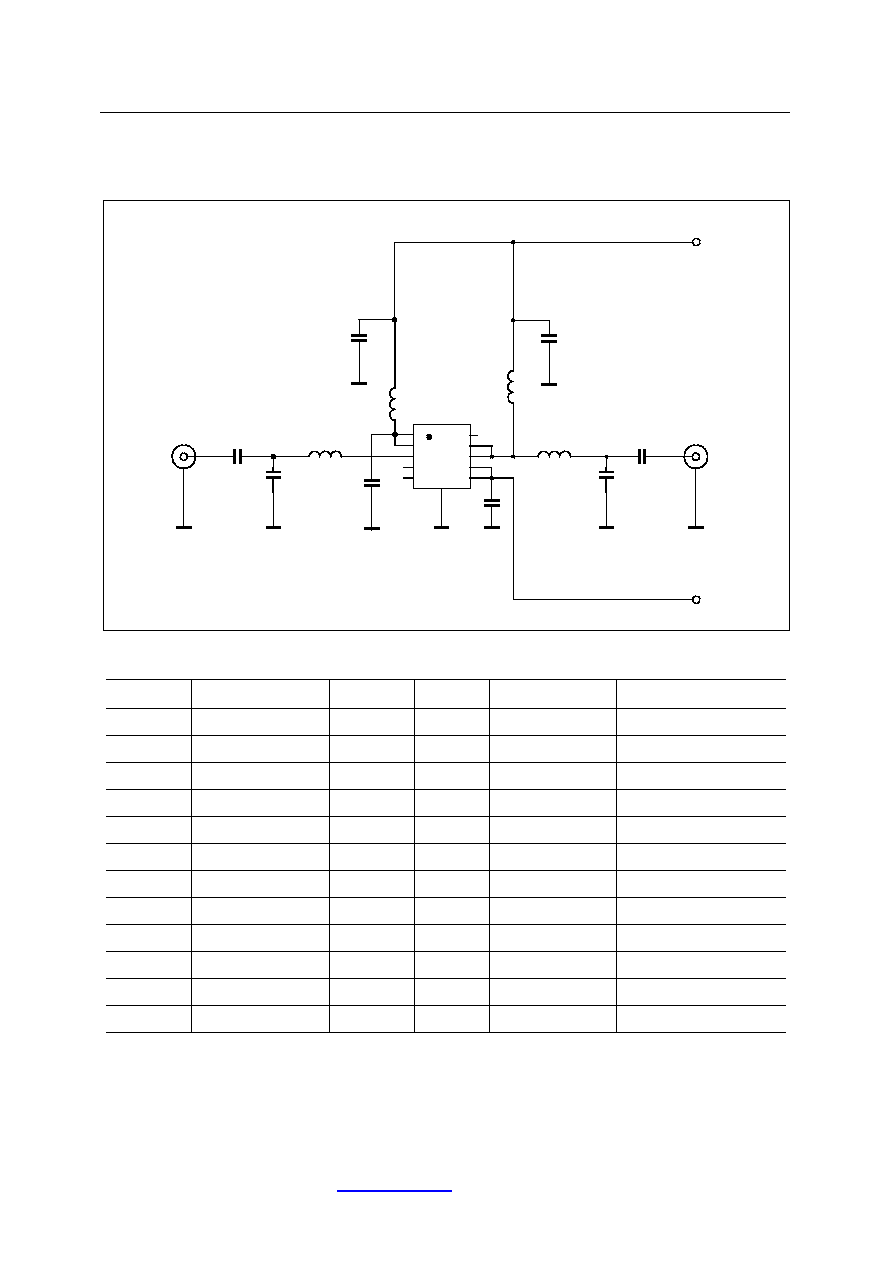
Application Note 2: Bluetooth Power Amplifier using Discrete Matching
RF In
RF Out
Vcc
Vctr
C1
C4
L2
CGB240
L1
L3
C7
C6
C3
C2
1
5
6
10
11
C8
L4
C5
Figure 5
Bluetooth Amplifier using discrete matching.
Part Type
Value
Outline
Source
Part
No.
C1
Cer. Capacitor
22 pF
0402
Murata COG
C2
Cer. Capacitor
22 pF
0402
Murata COG
C3
Cer. Capacitor
1.5 pF
0603
AVX ACCU-P
06035J1R5BBT
C4
Cer. Capacitor
2.0 pF
0402
Murata COG
C5
Cer. Capacitor
82 pF
0402
Murata COG
C6
Cer. Capacitor
0.1 µF
0603
Murata X7R
C7
Cer. Capacitor
1 nF
0402
Murata X7R
C8
Cer. Capacitor
0.1 µF
0603
Murata X7R
L1 Inductor 22
nH
0603
Toko
LL1005≠FH22NJ
L2 Inductor 1.0
nH
0402
Coilcraft 0402CS-1N0X_BG
L3 Inductor 1.0
nH
0402
Coilcraft 0402CS-1N0X_BG
L4 Inductor 22
nH
0603
Toko
LL1005≠FH22NJ
For further information please visit
www.triquint.com
pg.
11/13
Rev. 1.6 October 20th, 2004

CGB 240 Datasheet
TriQuint Semiconductor, Inc.
C6
C8
L
1
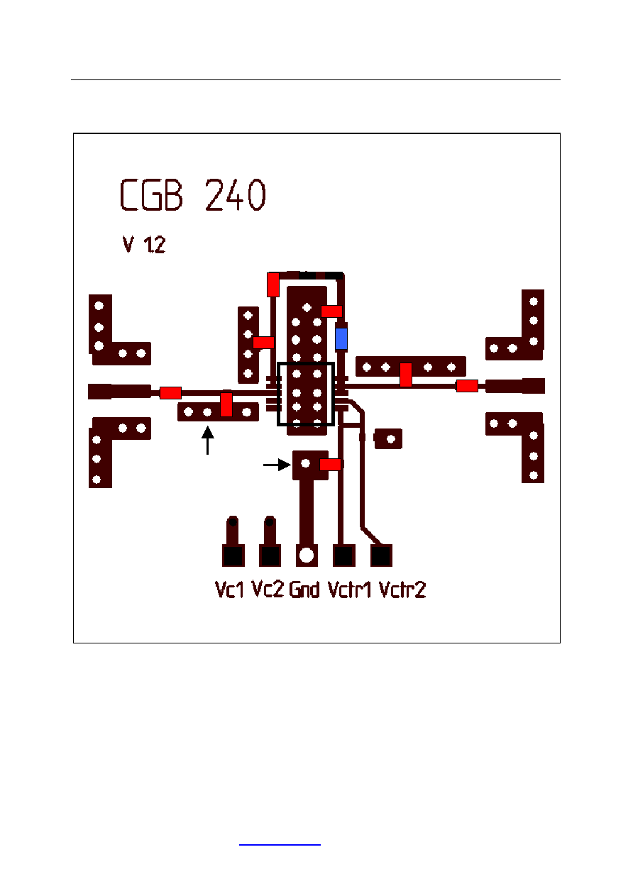
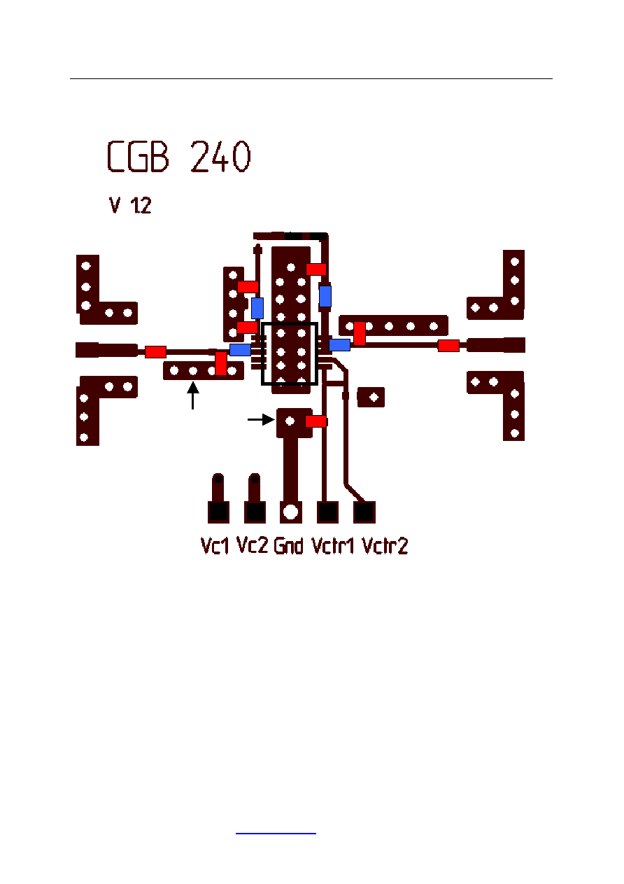
Figure 6
Layout of CGB240 Bluetooth evaluation board used in
application note 2.
For a discrete matching concept, the same evaluation board (V1.2) as shown in fig-
ure 5 might be used. However, to insert the series elements (L2, L3, L4), the pcb
lines have to be cut mechanically.
The use of a discrete matching concept saves pcb space but will lead to a lower out-
put power (typ. 0.3dB lower) and higher BOM cost.
CGB240
C1
C2
C
3
C
4
L
4
C5
L3
L2
,,White Dots" =
C7
Ground Vias
RF In
RF Out
(SMA)
(SMA)
For further information please visit
www.triquint.com
pg.
12/13
Rev. 1.6 October 20th, 2004

CGB 240 Datasheet
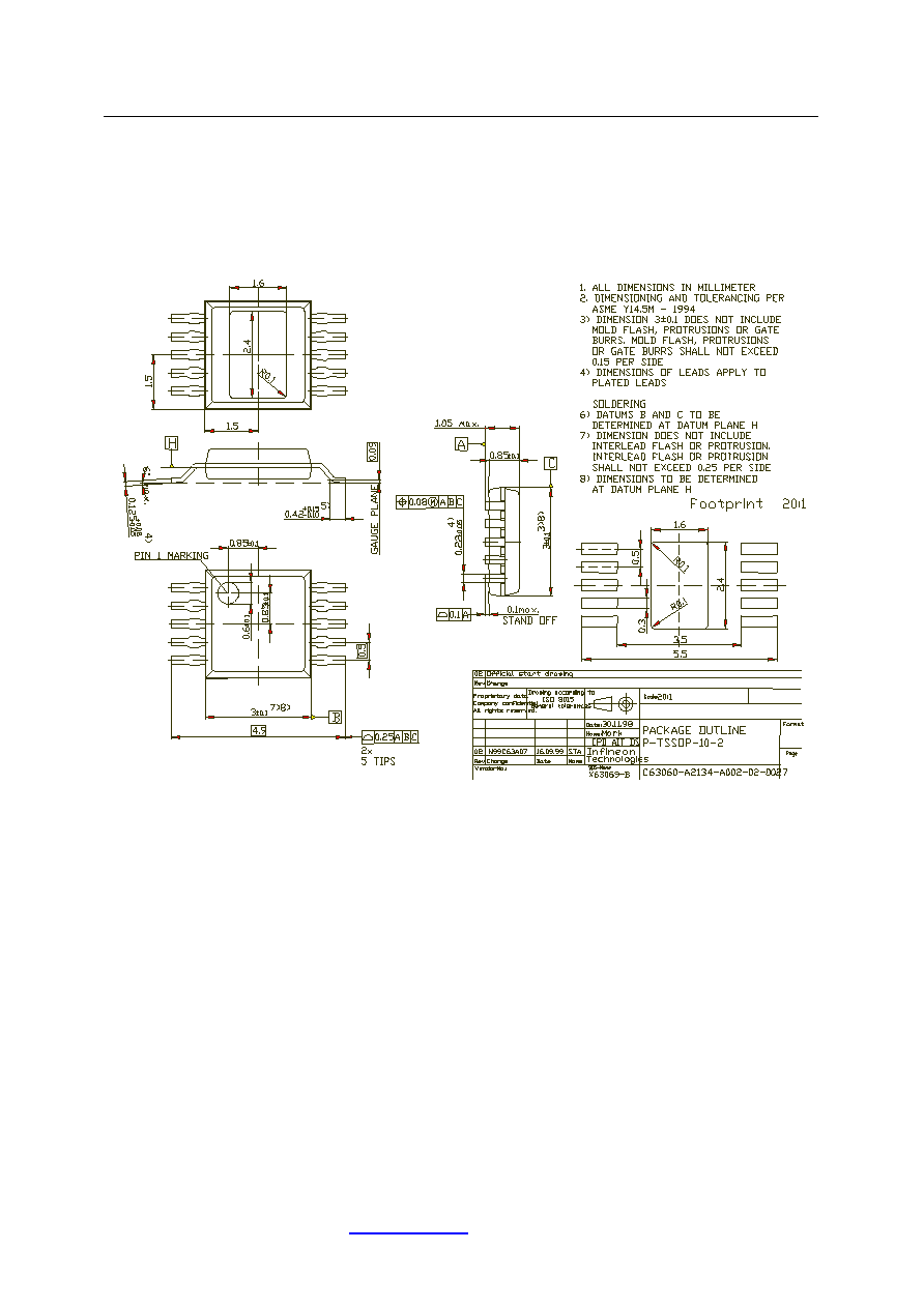
Description of MSOP-10 Package
In order to ensure maximum mounting yield and optimal reliability, special soldering condi-
tions apply in volume production. Please ask for our information brochure on details or
download the related document (TSSOP10_Soldering_Version01.pdf) from our website.
The TSSOP-10-2 is a level 1 package. International standards for handling this type of pack-
age are described in the JEDEC standard J-STD-033 ,,STANDARD FOR HANDLING,
PACKING, SHIPPING AND USE OF MOISTURE/REFLOW SENSITIVE SURFACE-MOUNT
DEVICES", published May-1999. The original document is available from the JEDEC website
www.jedec.org .
For further information please visit
www.triquint.com
pg.
13/13
Rev. 1.6 October 20th, 2004

CGB 240 Datasheet
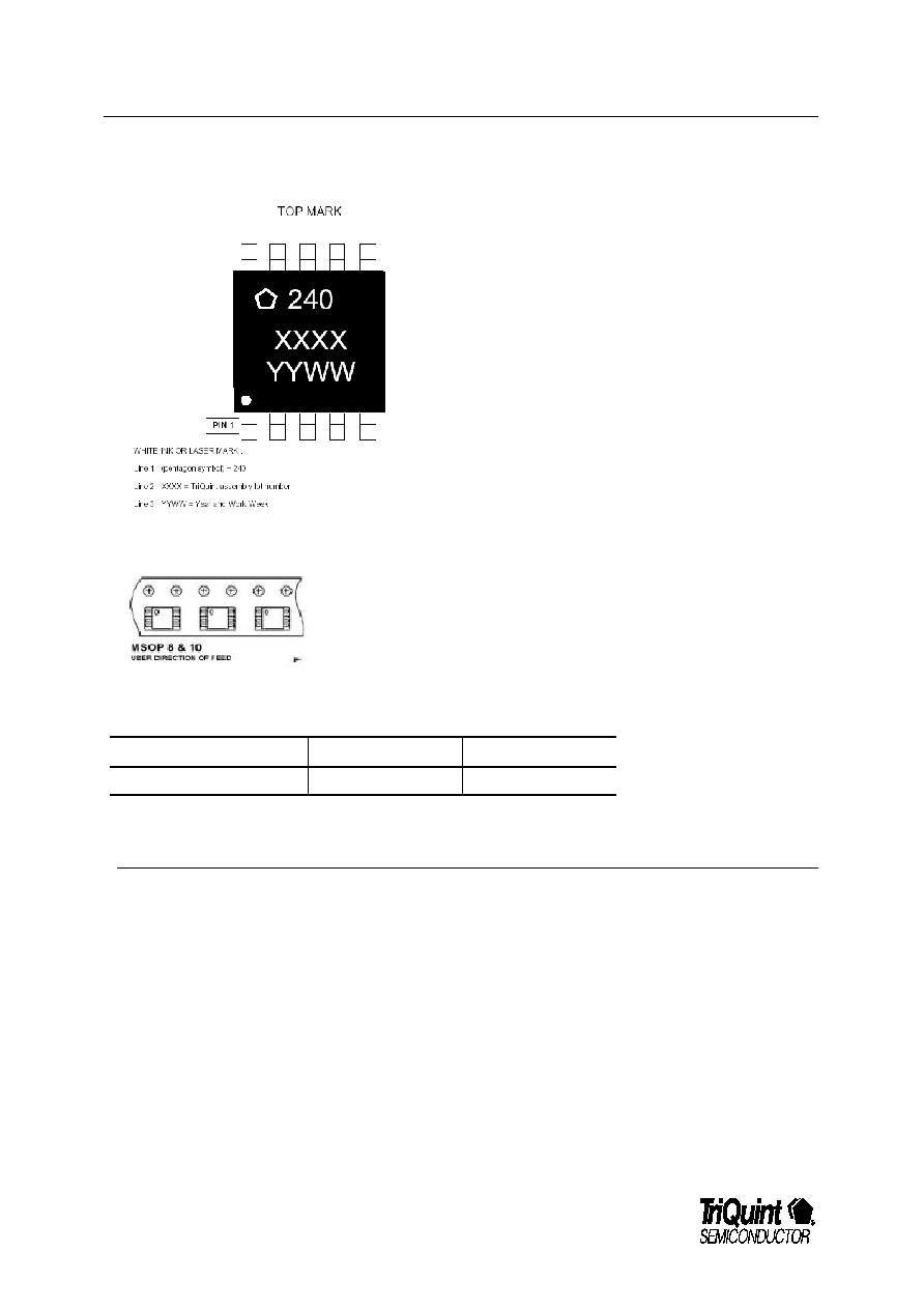
Part Marking:
Part Orientation on Reel:
Ordering Information:
Type Marking
Package
CGB240 CGB240
MSOP-10
ESD: Electrostatic discharge sensitive device
Observe handling precautions !
Additional Information
For latest specifications, additional product information, worldwide sales and distribution locations, and information about
TriQuint:
Web: www.triquint.com
Tel: (503) 615-9000
Email:
info_wireless@tqs.com
Fax: (503) 615-8902
For technical questions and additional information on specific applications:
Email:
info_wireless@tqs.com
The information provided herein is believed to be reliable; TriQuint assumes no liability for inaccuracies or omissions. TriQuint assumes no responsibility for
the use of this information, and all such information shall be entirely at the user's own risk. Prices and specifications are subject to change without notice. No
patent rights or licenses to any of the circuits described herein are implied or granted to any third party.
TriQuint does not authorize or warrant any TriQuint product for use in life-support devices and/or systems.
Copyright © 2003 TriQuint Semiconductor, Inc. All rights reserved.
Revision 1.5-December 16, 2003
For additional information and latest specifications, see our website: www.triquint.com
pg. 14/14

CGB 240 Datasheet
Additional Information
For latest specifications, additional product information, worldwide sales and distribution locations, and information about
TriQuint:
Web: www.triquint.com
Tel: (503) 615-9000
Email:
info_wireless@tqs.com
Fax: (503) 615-8902
For technical questions and additional information on specific applications:
Email:
info_wireless@tqs.com
The information provided herein is believed to be reliable; TriQuint assumes no liability for inaccuracies or omissions. TriQuint assumes no responsibility for
the use of this information, and all such information shall be entirely at the user's own risk. Prices and specifications are subject to change without notice. No
patent rights or licenses to any of the circuits described herein are implied or granted to any third party.
TriQuint does not authorize or warrant any TriQuint product for use in life-support devices and/or systems.
Copyright © 2003 TriQuint Semiconductor, Inc. All rights reserved.
Revision 1.5-December 16, 2003
For additional information and latest specifications, see our website: www.triquint.com
pg. 15/14
