 | –≠–ª–µ–∫—Ç—Ä–æ–Ω–Ω—ã–π –∫–æ–º–ø–æ–Ω–µ–Ω—Ç: CGB241 | –°–∫–∞—á–∞—Ç—å:  PDF PDF  ZIP ZIP |

CGB241
Data Sheet
2-Stage Bluetooth & WLAN InGaP HBT Power Amplifier
Applications:
∑
Bluetooth Class 1
∑
Home RF
∑
Cordless Phones
∑
IEEE 802.11b
∑
ISM-band Spread
Spectrum
Description:
The CGB241 GaAs Power Amplifier MMIC has been
especially developed for wireless applications in the
2.4 - 2.5 GHz ISM band (e.g. Bluetooth class 1, or
IEEE 802.11b). Its high power added efficiency (typi-
cally 50%) and single positive supply operation makes
the device ideally suited to handheld applications. The
device delivers 22.5 dBm output power at a supply volt-
age of 3.2 V, with an overall
PAE
of 50%. The output
power can be adjusted using an analog control voltage
(
V
CTR
). Simple external input-, interstage-, and output
matching circuits are used to adapt to the different re-
quirements of linearity and harmonic suppression in
various applications.
Package Outline:
Features:
∑
2-stage Bluetooth InGaP HBT power amplifier
∑
Single voltage supply
∑
Wide operating voltage range 2.0 - 5.5 V
∑ P
OUT
= 22.5 dBm at
V
C
= 3.2 V
∑
Overall power added efficiency (
PAE
) typically
50%
∑
Analog power control with four power steps
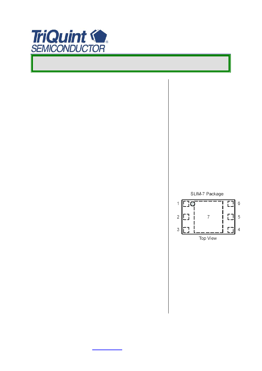
Pin Configuration:
1:
Vc1
2:
RFin
3:
NC
4:
Vcntrl1
5:
Vcntrl2
6:
Vc2
7 (paddle): GND
∑
High
PAE
at low≠power mode
∑
High harmonic suppression typ. 35 dBc
∑
Easy external matching concept
∑
Thin Small Leadless Package (
A
= 2.6mm
2
)
For further information please visit
www.triquint.com
pg.
1/14
Rev. A; November 14th, 2005.

CGB241
Data Sheet
2-Stage Bluetooth & WLAN InGaP HBT Power Amplifier
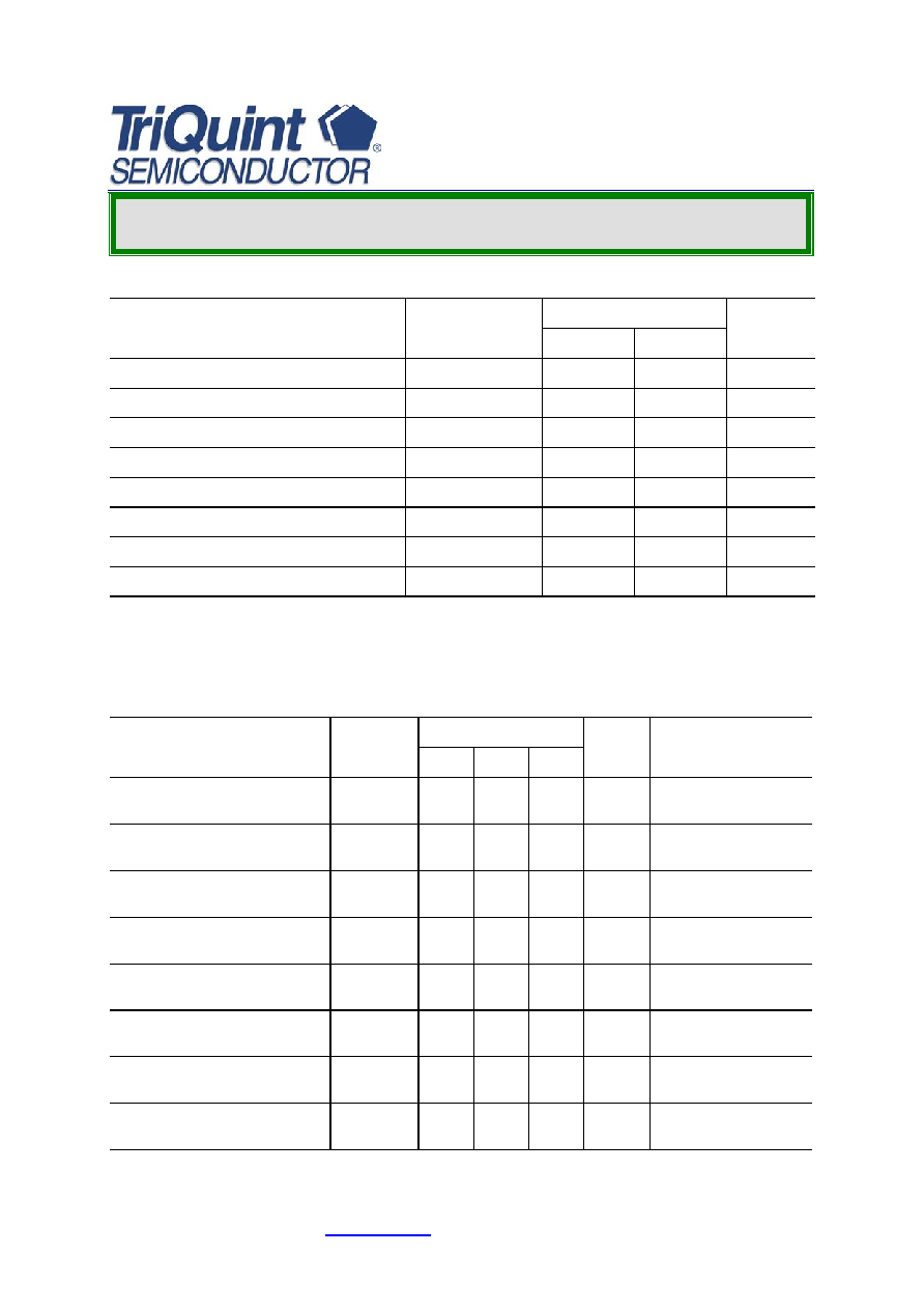
Absolute Maximum Ratings
Parameter Symbol
Limit
Values
Unit
min.
max.
Max. Supply Voltage
V
CC,MAX
0 5.5
V
Max. Control Voltage
V
CTR,MAX
0 3.2
V
Max. Current Stage 1
I
C1,MAX
0 40
mA
Max. Current Stage 2
I
C2,MAX
0 160
mA
Max. Total Power Dissipation
1
)
P
TOT
0.5
W
Max. RF Input Power
2
)
P
IN,MAX
+10
dBm
Channel Temperature
1
)
T
Ch
150
∞C
Storage Temperature
T
Stg
- 55
150
∞C
1
) Thermal resistance between junction and pad 7 ( = heatsink ):
R
THCH
= 100 K/W.
2
) No RF input signal should be applied at turn on of DC Power. An output VSWR of 1:1 is assumed.
Typical Electrical Characteristics in CGB241 Reference Design
T
A
= 25 ∞C;
V
CC
= 3.2 V;
f
= 2.4 ... 2.5 GHz;
Z
IN
=
Z
OUT
= 50 Ohms
Parameter
Symbol
Limit Values
Unit
Test Conditions
min
typ
max
Supply Current
Small-Signal Operation
I
CC,SS
120
150
mA
P
IN
= - 10 dBm
V
CTR
= 2.5 V
Power Gain
Small-Signal Operation
G
SS
24 26 dB
P
IN
= - 10 dBm
V
CTR
= 2.5 V
Output Power
Power Step 1
P
OUT,1
3
dBm
P
IN
= + 3 dBm
V
CTR
= 1.15 V
Supply Current
Power Step 1
I
CC,1
15
mA
P
IN
= + 3 dBm
V
CTR
= 1.15 V
Power Added Efficiency
Power Step 1
PAE
1
7
%
P
IN
= + 3 dBm
V
CTR
= 1.15 V
Output Power
Power Step 2
P
OUT,2
12
dBm
P
IN
= + 3 dBm
V
CTR
= 1.3 V
Supply Current
Power Step 2
I
CC,2
30
mA
P
IN
= + 3 dBm
V
CTR
= 1.3 V
Power Added Efficiency
Power Step 2
PAE
2
15
%
P
IN
= + 3 dBm
V
CTR
= 1.3 V
For further information please visit
www.triquint.com
pg.
2/14
Rev. A; November 14th, 2005.

CGB241
Data Sheet
2-Stage Bluetooth & WLAN InGaP HBT Power Amplifier
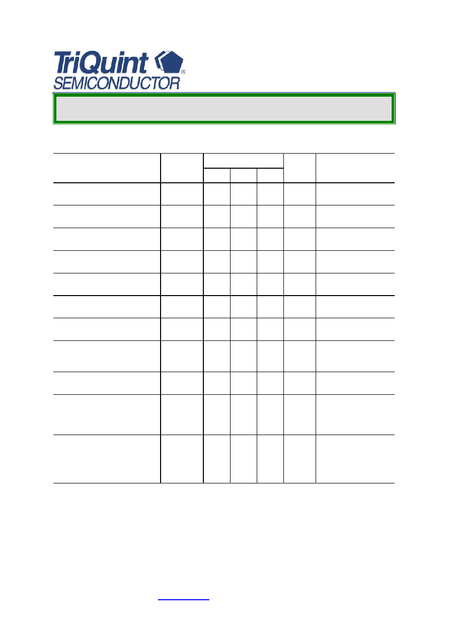
Electrical Characteristics in CGB241 Reference Design (cont.)
Parameter
Symbol
Limit Values
Unit
Test Conditions
Min
typ
max
Output Power
Power Step 3
P
OUT,3
17
dBm
P
IN
= + 3 dBm
V
CTR
= 1.5 V
Supply Current
Power Step 3
I
CC,3
52
mA
P
IN
= + 3 dBm
V
CTR
= 1.5 V
Power Added Efficiency
Power Step 3
PAE
3
30
%
P
IN
= + 3 dBm
V
CTR
= 1.5 V
Output Power
Power Step 4
P
OUT,4
22.0 22.5 dBm
P
IN
= + 3 dBm
V
CTR
= 2.5 V
Supply Current
Power Step 4
I
CC,4
130
170
mA
P
IN
= + 3 dBm
V
CTR
= 2.5 V
Power Added Efficiency
Power Step 4
PAE
4
40 50 - %
P
IN
= + 3 dBm
V
CTR
= 2.5 V
2
nd
Harm. Suppression
Power Step 4
h
2
-
35
-10
dBc
P
IN
= + 3 dBm
V
CTR
= 2.5 V
Turn-Off Current
I
CC,OFF
0.5
uA V
CC
= n/c
V
CTR
< -2.0 V
No RF Input
Off-State Isolation
S
21,0
26
dB
P
IN
= + 3 dBm
V
CTR
= 0 V
Stable Load VSWR
(no oscillation for any phase
of load)
VSWR
6
P
IN
= + 3 dBm
V
CC
= 3.2 V
V
CTR
= 2.5 V
Z
IN
= 50 Ohms
Maximum Load VSWR
(no damage to device)
allowed for 10s
RF must not be applied
before DC is turned on !
VSWR
6
P
IN
= + 5 dBm
V
CC
= 4.8 V
V
CTR
= 2.5 V
Z
IN
= 50 Ohms
For further information please visit
www.triquint.com
pg.
3/14
Rev. A; November 14th, 2005.

CGB241
Data Sheet
2-Stage Bluetooth & WLAN InGaP HBT Power Amplifier
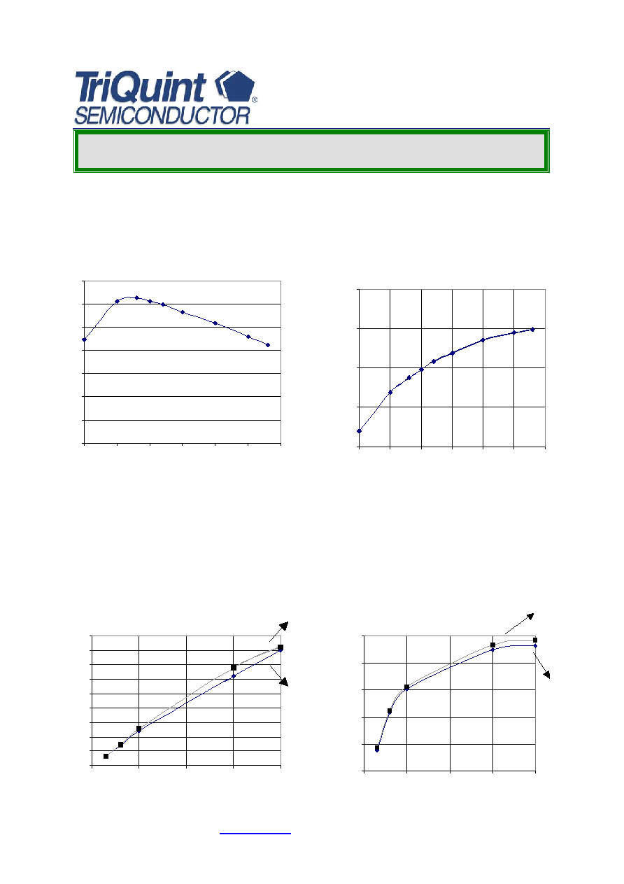
Typical Device Performance
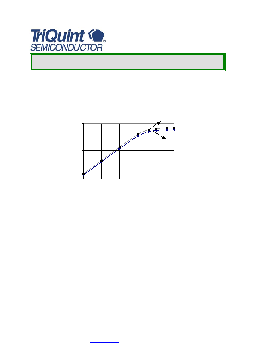
PAE versus Vcc
Pout versus Vcc
Vcntrl: 2.5V; Pin: +3 dBm @ 2.45 GHz
Vcntrl: 2.5V; Pin: +3 dBm @ 2.45
GHz
20
25
30
35
40
45
50
55
2
2.5
3
3.5
4
4.5
5
Vcc (V)
PAE (%)
19
21
23
25
27
2
2.5
3
3.5
4
4.5
5
Vcc (V)
Pout (dBm)
Supply Current
I
CC
=
f
(
V
CTR
) Output
Power
P
OUT
=
f
(
V
CTR
)
Icc vs Vctrl
Pin: 2.45GHz / +3dBm
0
20
40
60
80
100
120
140
160
180
1
1.5
2
2.5
3
Vctrl (V)
Icc (mA)
Vcc :2.8V
Vcc :3.2V
Pout vs Vctrl
Pin: 2.45 GHz / +3dBm
0
5
10
15
20
25
1
1.5
2
2.5
3
Vctrl(V)
Pout (dBm
)
Vcc :2.8V
Vcc :3.2V
For further information please visit
www.triquint.com
pg.
4/14
Rev. A; November 14th, 2005.

CGB241
Data Sheet
2-Stage Bluetooth & WLAN InGaP HBT Power Amplifier
Output Power Compression
P
OUT
=
f
(
P
IN
)
Pout vs Pin
Vctrl:2.5V, f(IN) :2.45GHz
5.0
10.0
15.0
20.0
25.0
-20
-15
-10
-5
0
5
Pin (dBm)
Pout (dBm)
Vcc :3.2V
Vcc :2.8V
For further information please visit
www.triquint.com
pg.
5/14
Rev. A; November 14th, 2005.

CGB241
Data Sheet
2-Stage Bluetooth & WLAN InGaP HBT Power Amplifier
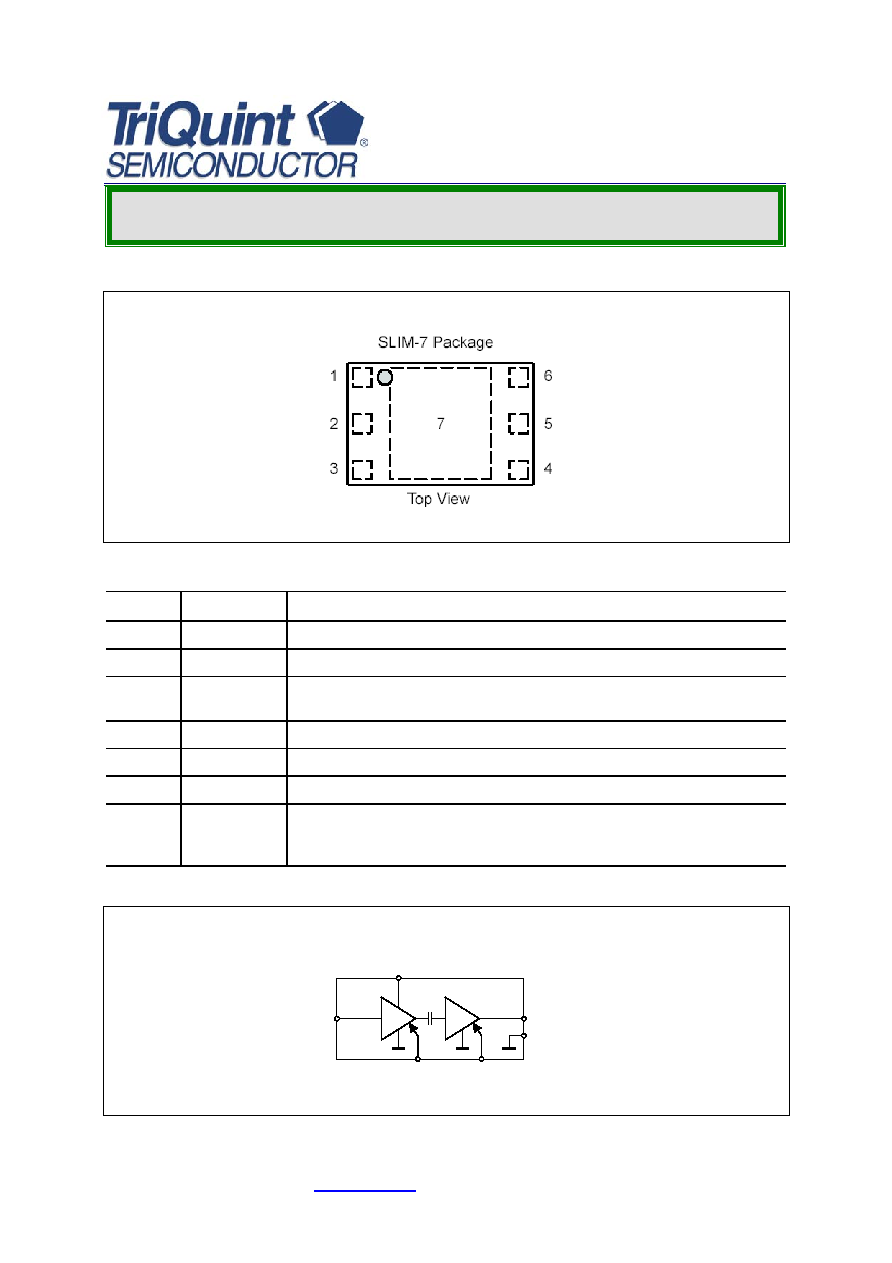
Pinning
Figure 1
CGB241 Outline: SLIM-7 Package
Pad Symbol Function
1 V
C1
Supply voltage of 1
st
stage / interstage match
2 RF
IN
RF input
3 NC
No connection; It is recommended to ground this pad as short as possi-
ble e.g. by a via under the pad.
4 V
CTR1
Control voltage 1
st
stage
5 V
CTR2
Control voltage 2
nd
stage
6 V
C2
Supply voltage of 2
nd
stage / RF output
7
GND
RF and DC ground (pad located on backside of package)
Heatsink. Thermal resistance between junction ≠ pad 7:
R
THCH
= 100
K/W.
Functional Diagram
(2)
RFin
(1)
Vc1
(6) Vc2
(7) Gnd
(4)
Vctr1
(5)
Vctr2
Figure 2
CGB241 Functional Diagram
For further information please visit
www.triquint.com
pg.
6/14
Rev. A; November 14th, 2005.

CGB241
Data Sheet
2-Stage Bluetooth & WLAN InGaP HBT Power Amplifier
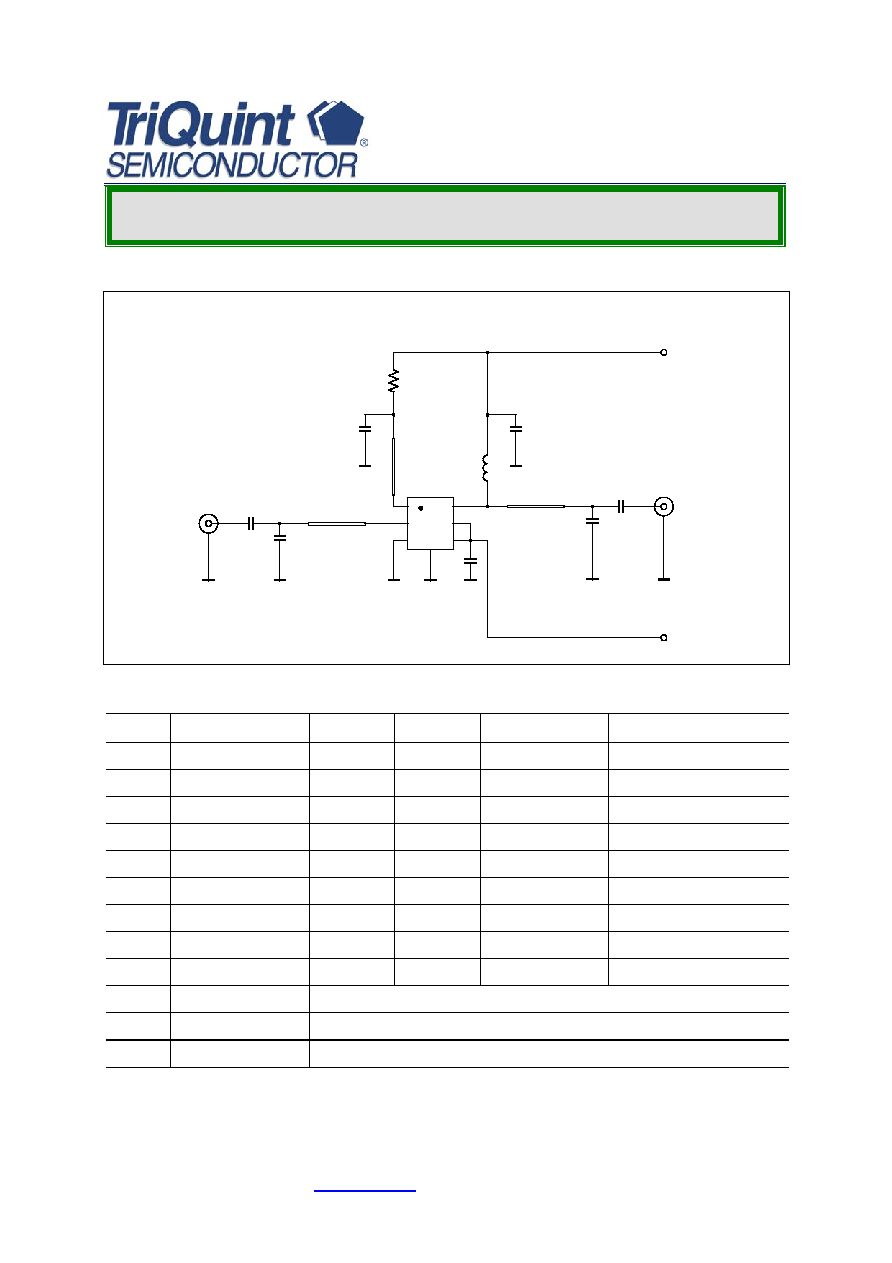
Application Note 1: CGB241 Reference Design
RF In
RF Out
Vcc
C1
C4
C5
TRL1
TRL2
CGB241
L1
TRL3
R1
C7
C6
C3
C2
1
3
4
5
2
6
Vctr
7
Figure 3
Schematic of CGB241 reference design.
Part Type
Value Outline Source
Part
No.
C1
Cer. Capacitor
22 pF
0402
Murata COG
C2
Cer. Capacitor
22 pF
0402
Murata COG
C3
4
)
Cer. Capacitor
1.5 pF
0603
AVX ACCU-P
06035J1R5BBT
C4
Cer. Capacitor
2.2 pF
0402
Murata COG
C5
Cer. Capacitor
10 pF
0402
Murata COG
C6
Cer. Capacitor
1 µF
0603
Murata X7R
C7
Cer. Capacitor
1 nF
0402
Murata X7R
L1 Inductor
22
nH 0603 Toko
LL1608≠FS
R1 Resistor
10
R 0402 Mira
TRL1 Microstrip
Line FR4 substrate;
h
= 0,2 mm;
w
= 0,32 mm
TRL2 Microstrip
Line FR4 substrate;
h
= 0,2 mm;
w
= 0,32 mm
TRL3 Microstrip
Line FR4 substrate;
h
= 0,2 mm;
w
= 0,32 mm
4
) Cost optimization might take place by using lower-Q AVX-CU capacitors instead of the AccuP ver-
sion. This will lead to better
h
2
performance, however resulting in a loss of about 2% PAE. Line length
l
is the total distance from the corner of tuning capacitor to the corner of MMIC's package. Length of
bend structures measured in the middle of the corresponding conductor.
For further information please visit
www.triquint.com
pg.
7/14
Rev. A; November 14th, 2005.

CGB241
Data Sheet
2-Stage Bluetooth & WLAN InGaP HBT Power Amplifier
TriQuint Semiconductor, Inc.
R
1
C1
C7
C5
C
4
L
1
,,White Dots" =
Ground Vias
CGB
241
C6
C
3
C2
RF Out
(SMA)
RF In
(SMA)
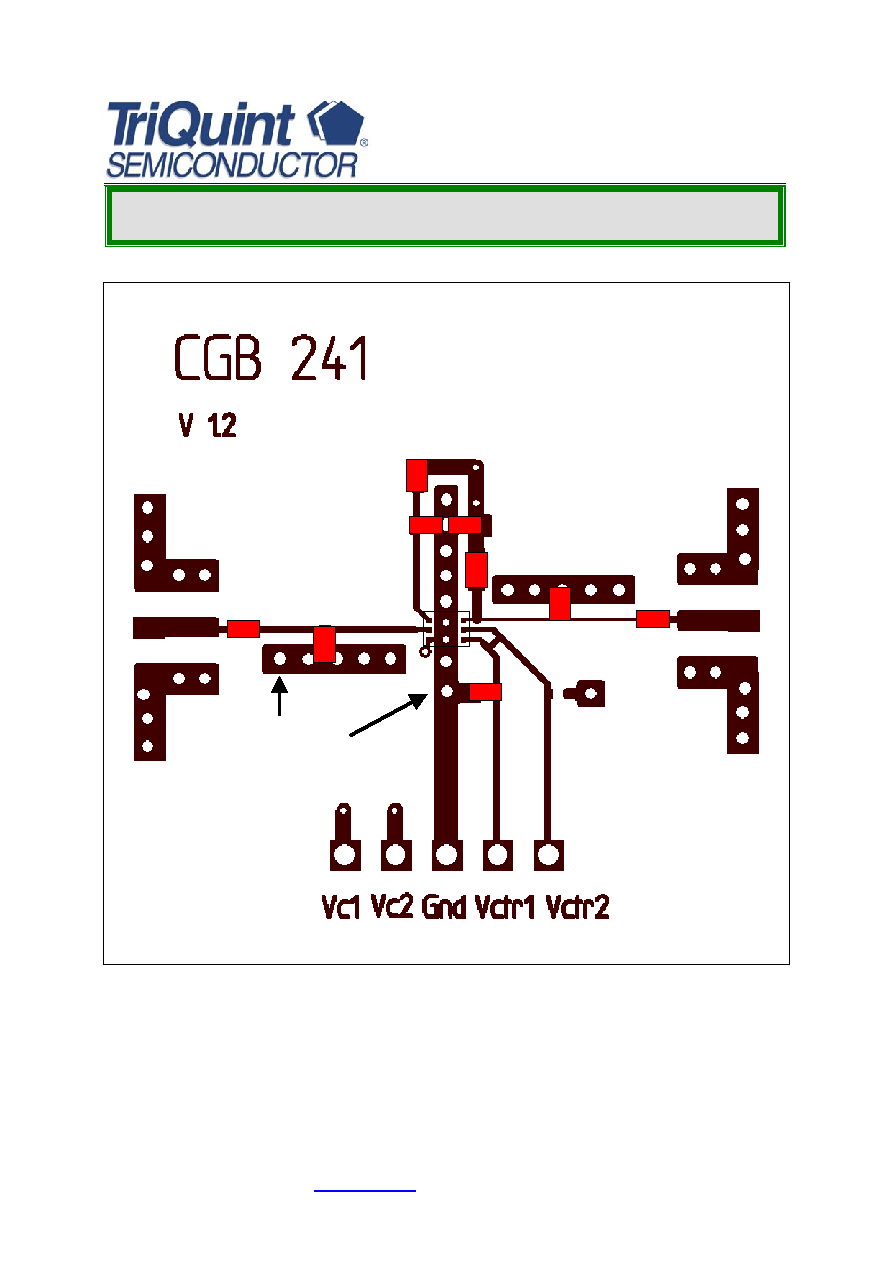
Figure 4
Layout of CGB241 reference design.
Notes:
Vc1 and Vc2 are connected together on the PCB.
Vctr1 and Vctr2 are connected together on the PCB.
For further information please visit
www.triquint.com
pg.
8/14
Rev. A; November 14th, 2005.

CGB241
Data Sheet
2-Stage Bluetooth & WLAN InGaP HBT Power Amplifier
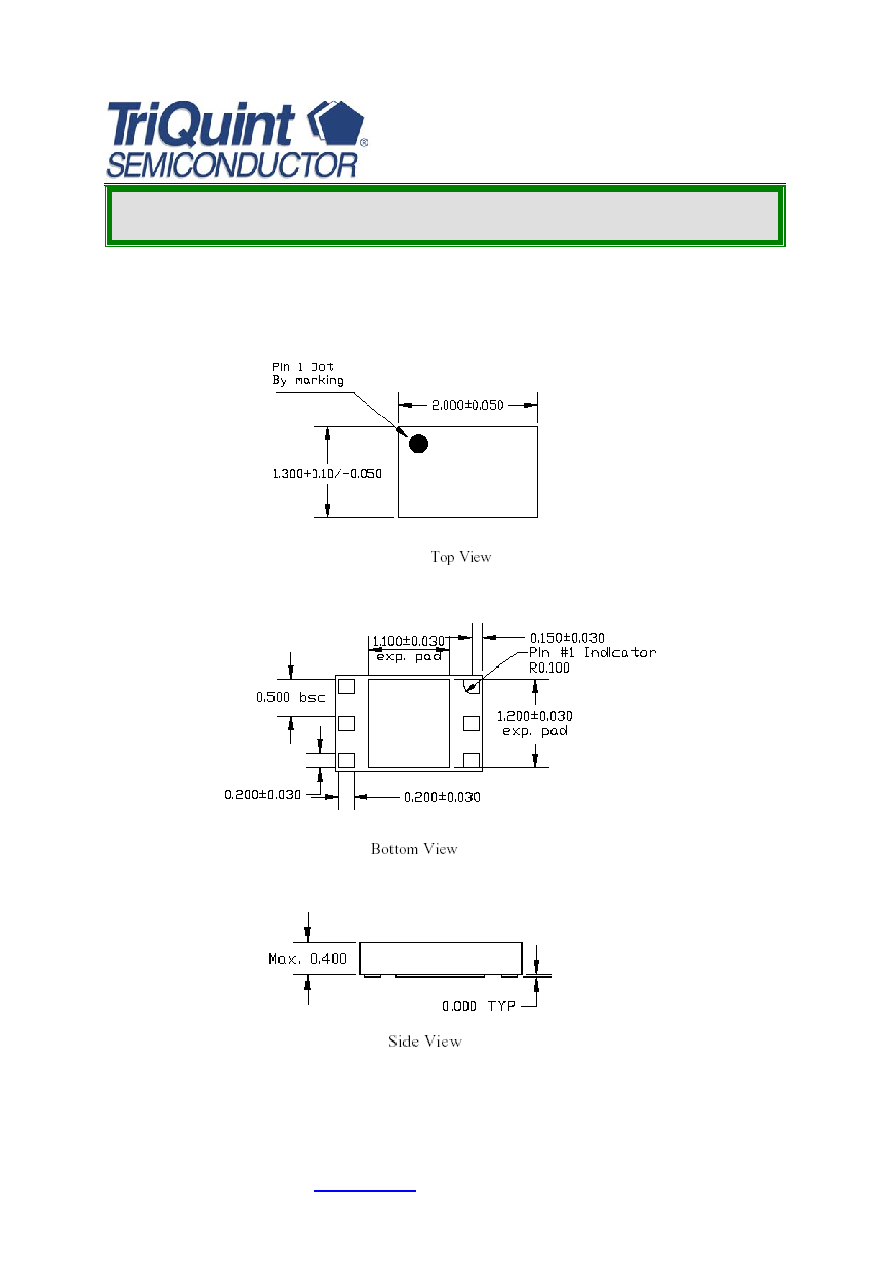
Package Outline of SLIM-7 Package
For further information please visit
www.triquint.com
pg.
9/14
Rev. A; November 14th, 2005.

CGB241
Data Sheet
2-Stage Bluetooth & WLAN InGaP HBT Power Amplifier
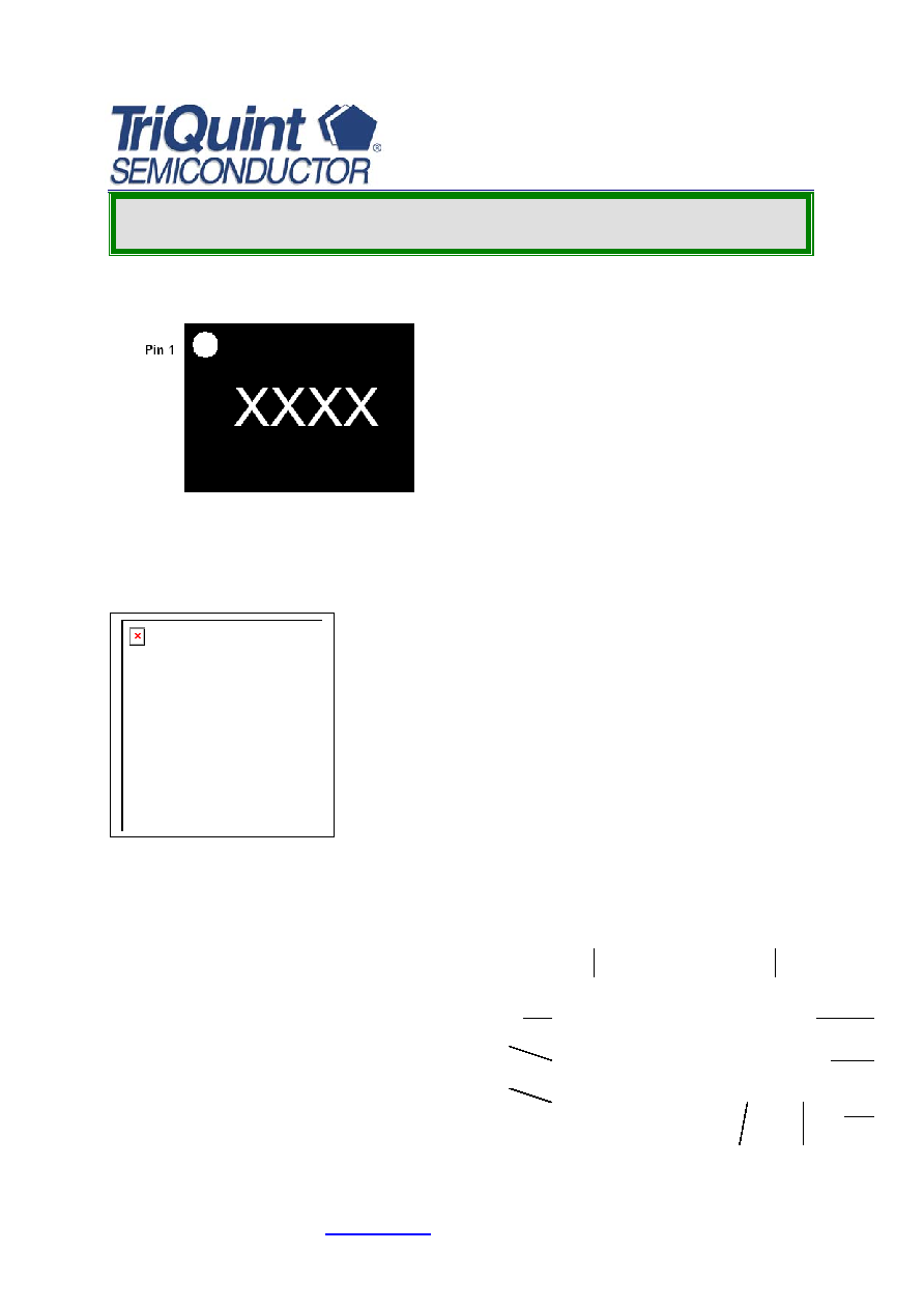
Part Marking:
White Ink or Laser Mark; XXXX = last 4 digits of lot code.
Product Label:
8
9
10
6
7
For further information please visit
www.triquint.com
pg.
10/14
Rev. A; November 14th, 2005.

CGB241
Data Sheet
2-Stage Bluetooth & WLAN InGaP HBT Power Amplifier
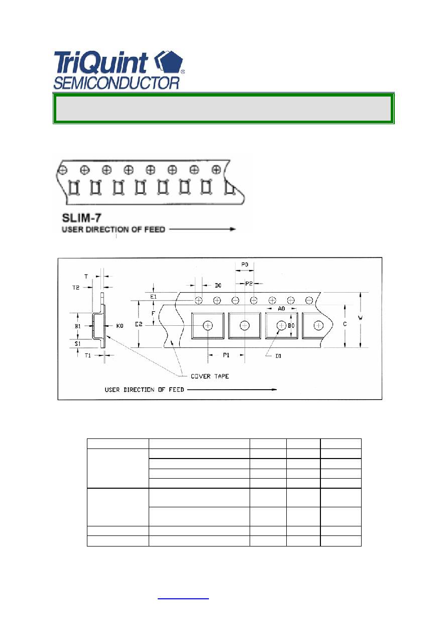
Tape and Reel Information:
PART
FEATURE
SYMBOL SIZE (in) SIZE (mm)
LENGTH A0
0.062
1.57
WIDTH B0
0.087
2.21
DEPTH K0
0.023
0.59
CAVITY
PITCH P1
0.157
4.00
CAVITY TO PERFORATION
LENGTH DIRECTION
P2 0.079
2.00
DISTANCE
BETWEEN
CENTERLINE
CAVITY TO PERFORATION
WIDTH DIRECTION
F 0.138
3.50
COVER TAPE
WIDTH
C
0.213
5.40
CARRIER TAPE WIDTH
W
0.315
8.00
For further information please visit
www.triquint.com
pg.
11/14
Rev. A; November 14th, 2005.

CGB241
Data Sheet
2-Stage Bluetooth & WLAN InGaP HBT Power Amplifier
Carton Label:
For further information please visit
www.triquint.com
pg.
12/14
Rev. A; November 14th, 2005.

CGB241
Data Sheet
2-Stage Bluetooth & WLAN InGaP HBT Power Amplifier
Packing List Label:
For further information please visit
www.triquint.com
pg.
13/14
Rev. A; November 14th, 2005.

CGB241
Data Sheet
2-Stage Bluetooth & WLAN InGaP HBT Power Amplifier
Ordering Information:
Type Marking
Package
CGB241 XXXX
SLIM-7
ESD: Electrostatic discharge sensitive device
Observe handling precautions!
Moisture: The CGB241 is rated Moisture Sensitivity Level 1 at 260∫C per JEDEC
Standard IPC/JEDEC J-STD-020.
RoHS: The CGB241 is compliant with RoHS Directive (Restrictions on the use of
certain Hazardous Substances in Electrical and Electronic Equipment).
Additional Information
For latest specifications, additional product information, worldwide sales and distribution locations, and information about
TriQuint:
Web: www.triquint.com
Tel: (503) 615-9000
Email:
info_wireless@tqs.com
Fax: (503) 615-8902
For technical questions and additional information on specific applications:
Email:
info_wireless@tqs.com
The information provided herein is believed to be reliable; TriQuint assumes no liability for inaccuracies or omissions. TriQuint assumes no responsibility for
the use of this information, and all such information shall be entirely at the user's own risk. Prices and specifications are subject to change without notice. No
patent rights or licenses to any of the circuits described herein are implied or granted to any third party.
TriQuint does not authorize or warrant any TriQuint product for use in life-support devices and/or systems.
Copyright © 2003 TriQuint Semiconductor, Inc. All rights reserved.
Revision 1.4- ,December 12th, 2003
For additional information and latest specifications, see our website: www.triquint.com
For further information please visit
www.triquint.com
pg.
14/14
Rev. A; November 14th, 2005.
