 | –≠–ª–µ–∫—Ç—Ä–æ–Ω–Ω—ã–π –∫–æ–º–ø–æ–Ω–µ–Ω—Ç: CMH0819N | –°–∫–∞—á–∞—Ç—å:  PDF PDF  ZIP ZIP |

CMH0819 - Final Datasheet (October 1st, 2002)
1
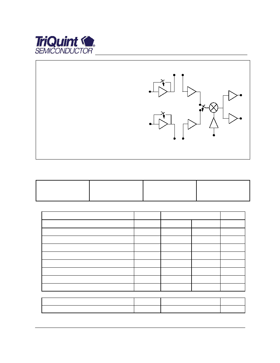
GaAs MMIC CMH0819
∑
High-Linearity, Dual-Band LNA/Mixer IC for
use in CDMA and TDMA Mobile Phones
∑
Integrated bypass switch for LNAs
∑
GaAs PHEMT Process
∑
Leadless 3.5 x 4.5 mm. SMT package
∑
LO Input power range: -7.0 to 0 dBm
∑
Operating voltage range: 2.7 to 4 V
∑
Total current consumption: 19 mA
ESD: Electrostatic discharge sensitive device
Observe handling Precautions!
Type
Marking
Ordering code
(tape and reel)
Package
CMH0819
0819
TBD
VQFN-24
Maximum Ratings
Symbol
Value
Unit
min
max
Supply Voltage
VDD
0
6
V
DC-Voltage at RF Ports
VRF
- 0.3
0.3
V
DC-Voltage at GND Ports
VGND
- 0.3
0.3
V
DC-Voltage at CNTL Ports
VCNTL
0
0.3 + VDD
V
Power into LO Inputs
Pin,LO
10
dBm
Operating Temperature
T
a
-40
85
∞C
Channel Temperature
TCh
150
∞C
Storage Temperature
Tstg
-55
150
∞C
Thermal Resistance
Channel to Soldering Point (GND)
RthChS
141
∞C /W
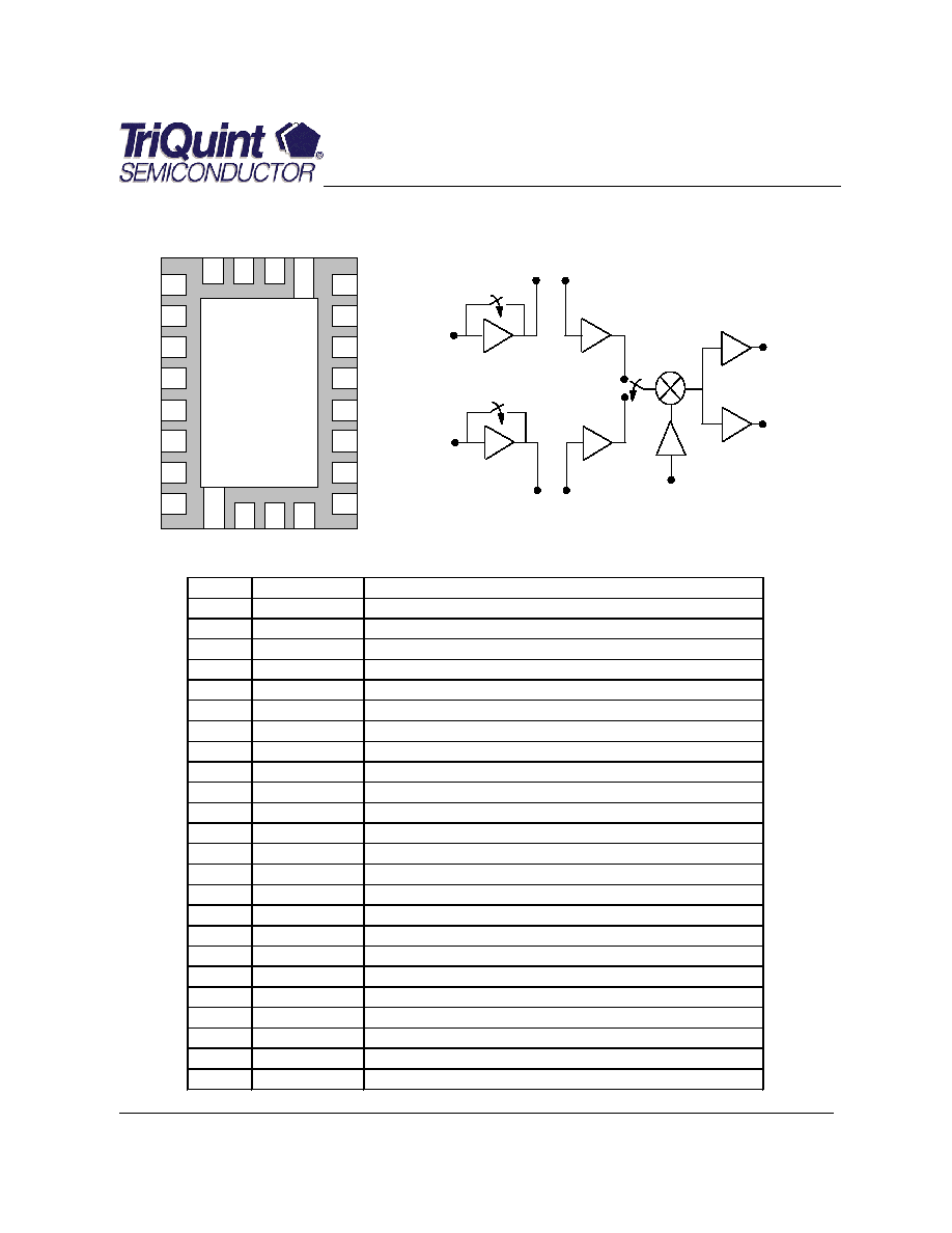
IF
OUT
AMPS
CDMA
Dual-Band
LO Input
LNA
LNA
CELLULAR
PCS
Filter
Ports
Filter
Ports

CMH0819 - Final Datasheet (October 1st, 2002)
2
GaAs MMIC CMH0819
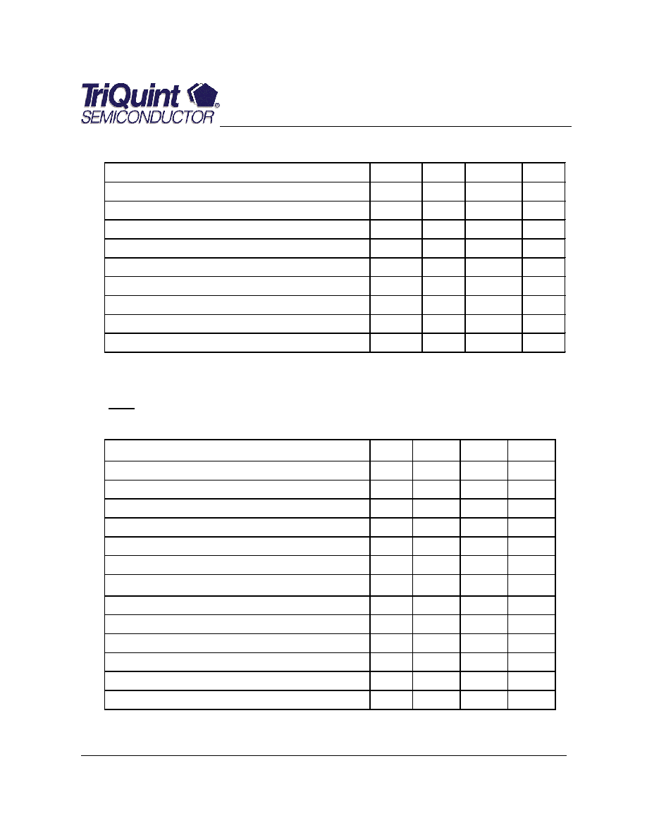
Electrical Characteristics
Parameter min
typ
max
Unit
RF - Frequency range 1 (Cellular)
869
-
894
MHz
LO - Frequency range 1
(1)
919
-
1144
MHz
RF - Frequency range 2 (PCS)
1930
-
1990
MHz
LO - Frequency range 2
(1)
1980
-
2240
MHz
IF Frequency range
50
-
250
MHz
LO Power Input
-7.0
-
0.0
dBm
Supply Voltage (Vdd)
2.7
-
4.0
V
High Logic Level (H)
VDD -0.2
2.7
0.3 + VDD V
Low Logic Level (L)
0.0
-
0.2
V
1) Low-side LO can be achieved using external tuning
LNA ≠ Performance of LNA section
Test conditions: T
a
= 25∞C, V
DD
= 2.7 V
Mode ≠ Cellular, High Gain
min
typ
max
Unit
Operating Current
5
mA
Noise Figure
1.1
1.5
dB
Gain 12.0
13.2
14.5
dB
3rd Order Input Intercept Point
7.0
9.0
dBm
Input return loss
13
dB
Output return loss
15
dB
Mode ≠ Cellular, Low Gain
min
typ
max
Unit
Operating Current
0
mA
Noise Figure
4.0
5.0
dB
Gain -4.5
-3.5
-2.5
dB
3rd Order Input Intercept Point
22
28
dBm
Input return loss
13
dB
Output return loss
15
dB

CMH0819 - Final Datasheet (October 1st, 2002)
3
GaAs MMIC CMH0819
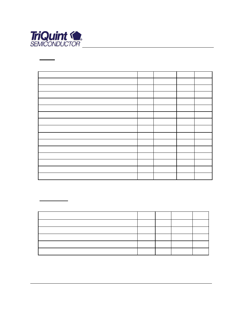
LNA ≠ Performance of LNA section (continued)
Test conditions: T
a
= 25∞C, V
DD
= 2.7 V
Mode ≠ PCS, High Gain
min
typ
Max
Unit
Operating Current
5.5
mA
Noise Figure
1.1
1.5
dB
Gain 11.5
13
14.3
dB
3rd Order Input Intercept Point
7.0
9.0
dBm
Input return loss
10
dB
Output return loss
15
dB
Mode ≠ PCS, Low Gain
min
typ
max
Unit
Operating Current
0
mA
Noise Figure
4.0
5.0
dB
Gain -4.0
-3.0
-2.0
dB
3rd Order Input Intercept Point
22
28
dBm
Input return loss
12
dB
Output return loss
12
dB
MIXER - Electrical Characteristics of Mixer section
Test conditions:
Ta = 25∞C; VDD= 2.7V, PLO = -7 dBm
,
f
LO
= f
RF
+ f
IF
, fIF = 130MHz
Mode ≠ Cellular, CDMA
min
typ
max
Unit
Operating Current
15.5
mA
Conversion Gain
15.0
17.3
19.0
dB
Noise Figure
4.2
5.5
dB
3rd Order Input Intercept Point
4.5
7.0
dBm
RF Input return loss
10
dB
LO Input return loss
10
dB
IF Output Impedance
(1)
900-j*800
1) IF Output externally tuned to match IF SAW filter

CMH0819 - Final Datasheet (October 1st, 2002)
4
GaAs MMIC CMH0819
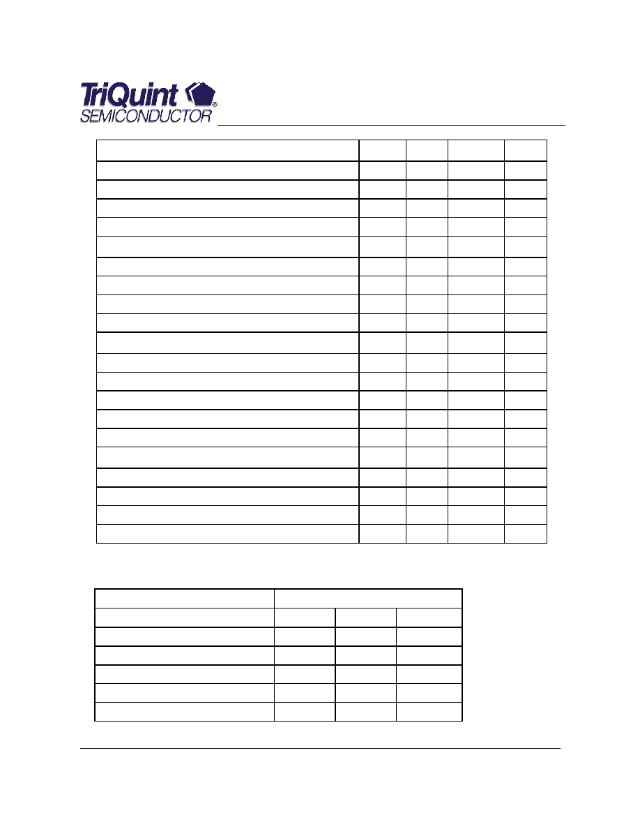
MIXER - Electrical Characteristics of Mixer section (continued)
Test conditions:
Ta = 25∞C; VDD= 2.7V, PLO = -7 dBm
,
f
LO
= f
RF
+ f
IF
, fIF = 130MHz
Mode ≠ Cellular, AMPS
min
typ
max
Unit
Operating Current
11.5
mA
Conversion Gain
6.7
9
11.2
dB
Noise Figure
5.5
7.5
dB
3rd Order Input Intercept Point
3.0
6.0
dBm
RF Input return loss
10
dB
LO Input return loss
10
dB
IF Output Impedance
(1)
142-j*40
Mode ≠ PCS, CDMA
min
typ
max
Unit
Operating Current
16.0
mA
Conversion Gain
15.5
17.5
19.7
dB
Noise Figure
4.6
6.0
dB
3rd Order Input Intercept Point
2.0
4.0
dBm
RF Input return loss
10
dB
LO Input return loss
10
dB
IF Output Impedance
(1)
900 - j*800
1) IF Output externally tuned to match IF SAW filter
FULL CHAIN ≠ LNA / Downconverter Performance
Test conditions: Ta = 25 ∞C, VDD= 2.7 V, PLO = -7 dBm
,
fIF = 130 MHz
Mode ≠ Cellular, High Gain, CDMA
min
typ
max
Unit
Total operating Current
20.5
26.5
mA
Conversion Gain
(2)
27
dB
Noise Figure
1.7
dB
Input IP3
-3.8
dBm
LNA Input IP3
9.0
dBm
2) Assumes 3.0 dB loss for image filter

CMH0819 - Final Datasheet (October 1st, 2002)
5
GaAs MMIC CMH0819
Electrical Characteristics ≠ LNA / Downconverter (continued)
Mode ≠ Cellular, Low Gain, CDMA
min
typ
max
Unit
Total operating Current
15.5
19.1
mA
Conversion Gain
(2)
10
dB
Noise Figure
11
dB
Input IP3
12.8
dBm
Mode ≠ Cellular, High Gain, AMPS
min
typ
max
Unit
Total operating Current
15.5
22.5
mA
Conversion Gain
(2)
19
dB
Noise Figure
2.0
dB
Input IP3
-4.7
dBm
Mode ≠ PCS, High-Gain, CDMA
min
typ
max
Unit
Total operating Current
21.5
27.0
mA
Conversion Gain
(2)
28.0
dB
Noise Figure
1.7
dB
Input IP3
-6.7
dBm
LNA Input IP3
8.0
dBm
Mode ≠ PCS, Low-Gain, CDMA
min
typ
max
Unit
Total operating Current
16
19.6
mA
Conversion Gain
(2)
11.0
dB
Noise Figure
11.0
dB
Input IP3
10.1
dBm
2) Assumes 3.0 dB loss for image filter
Truth Table
Control Voltage
Operating Mode
Band Sel
Gain Ctl
IF Select
Cellular, High Gain, CDMA
L
H
L
Cellular, Low Gain, CDMA
L
L
L
Cellular, Low Gain, AMPS
L
L
H
PCS, High Gain, CDMA
H
H
L
PCS, Low Gain, CDMA
H
L
L

CMH0819 - Final Datasheet (October 1st, 2002)
6
GaAs MMIC CMH0819
1
2
3
4
5
6
7
8
20
19
18
17
16
15
14
13
9 10 11 12
24 23 22 21
PIN
Symbol
Description
1
Vdd
Supply voltage
2
Vdd
Supply voltage
3
Band_sel
Band select control voltage
4
Pmix_in
Mixer 2 input from image filter (PCS band)
5
Vdd
Supply voltage
6
GND
Ground
7
Gain_cntl
Control voltage for LNA gain selection
8
Plna_out
RF output of LNA 2 (PCS band)
9
GND
Ground
10
Plna_in
RF Input to LNA 2 (PCS band)
11
Clna_in
RF Input to LNA 1 (Cellular band)
12
GND
Ground
13
Clna_out
RF output of LNA 1
14
Vdd
Supply voltage
15
Vdd
Supply voltage
16
Cmix_in
Mixer 1 input from image filter (Cellular band)
17
Mix_out
Mixer output (external match)
18
IFA_In
IF Amplifier Input
19
IFA_src
IF Amplifier FET source ground
20
AMPS_out
AMPS IF output
21
GND
Ground
22
CDMA_out
CDMA IF output
23
IF_Sel
IF Select (CDMA or AMPS)
24
LO_in
LO Input (Cellular and PCS bands)
PIN Assignments & Functional Block Diagram
IF
OUT
AMPS
CDMA
Dual-Band
LO Input
LNA
LNA
CELLULAR
PCS
Filter
Ports
Filter
Ports

CMH0819 - Final Datasheet (October 1st, 2002)
7
GaAs MMIC CMH0819
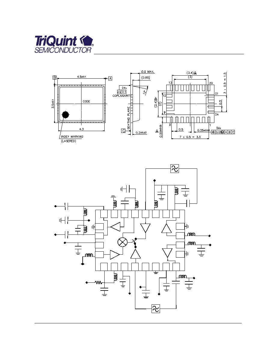
Package Outline - VQFN 24
Application Circuit
1
2
3
4
5
6
7
8
20
19
18
17
16
15
14
13
9
10
11
12
24
23
22
21
L6
L5
Vdd
L7
L8
C12
C13
C14
C15
C16
L9
L10
L1
Vdd
C1
L2
Clna_In
Plna_In
C5
Gain
C4
C3||C19
Vdd
Vdd
C6
C7
Band
Vdd
L3
L4
C8
IF_Sel
LO In
C17
C10||C21
C9
CDMA Out
AMPS Out
R1
C18
L11
(50 Ohm IF output )
C20

CMH0819 - Final Datasheet (October 1st, 2002)
8
GaAs MMIC CMH0819
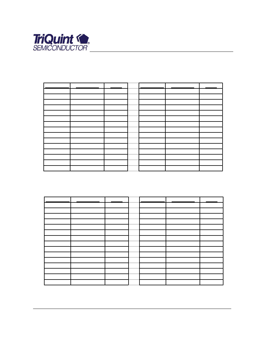
External Components
f
LO
= f
RF
+ f
IF
, f
IF
= 130MHz
Component
Description
Type
Component
Description
Type
C1
CAP, 0.5 PF
0402
C20
CAP, 3.3 PF
0402
C3,C4
CAP, 12 PF
0402
C21
CAP, 3.3 nF
0402
C5,C6
CAP, 100 PF
0402
R1
RES, 82 ohms
0402
C7
CAP, 1K PF
0402
R2,R3,R4
RES, 51K ohms
0402
C8
CAP, 100 PF
0402
L1
IND, 19 NH
0402
C9
CAP, 4.7 PF
0402
L2
IND, 6.2 nH
0402
C10
CAP, 0.1 uF
0402
L3
IND, 12 nH
0402
C12
CAP, 100 PF
0402
L4
IND, 4.7 nH
0402
C13
CAP, 5 PF
0402
L5
IND, 180 nH
0603
C14
CAP, 47 nF
0402
L6
IND, 120 nH
0603
C15
CAP, 51 PF
0402
L7
IND, 82 nH
0402
C16
CAP, 1.5 PF
0402
L8
IND, 180 nH
0603
C17
CAP, 15 PF
0402
L9
IND, 12 nH
0402
C18
CAP, 1.0 PF
0402
L10
IND, 12 nH
0402
C19
CAP, 0.1 uF
0402
L11
IND, 3.3 nH
0402
External Components,
f
LO
= f
RF
+ f
IF
, f
IF
= 184 MHz
Component
Description
Type
Component
Description
Type
C1
CAP, 0.5 PF
0402
C20
n/a
-
C3,C4
CAP, 12 PF
0402
C21
CAP, 3.3 nF
0402
C5,C6
CAP, 100 PF
0402
R1
RES, 82 ohms
0402
C7
CAP, 1K PF
0402
R2,R3,R4
RES, 51K ohms
0402
C8
CAP, 100 PF
0402
L1
IND, 19 NH
0402
C9
CAP, 3 PF
0402
L2
IND, 6.2 nH
0402
C10
CAP, 0.1 uF
0402
L3
IND, 12 nH
0402
C12
CAP, 100 PF
0402
L4
IND, 4.7 nH
0402
C13
CAP, 3.3 PF
0402
L5
IND, 180 nH
0603
C14
CAP, 47 nF
0402
L6
IND, 82 nH
0603
C15
CAP, 51 PF
0402
L7
IND, 68 nH
0402
C16
CAP, 1.5 PF
0402
L8
IND, 120 nH
0603
C17
CAP, 9 PF
0402
L9
IND, 12 nH
0402
C18
CAP, 1.0 PF
0402
L10
IND, 12 nH
0402
C19
CAP, 0.1 uF
0402
L11
IND, 3.3 nH
0402

CMH0819 - Final Datasheet (October 1st, 2002)
9
GaAs MMIC CMH0819
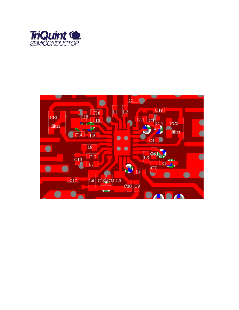
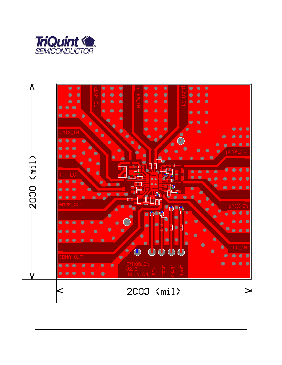
Recommended PCB Layout

CMH0819 - Final Datasheet (October 1st, 2002)
10
GaAs MMIC CMH0819
Evaluation Board
CM
H
0
81
9
C1
C3
C4
C6
C7
R1
L3
L4
C5
C9
L5
C10
L6
L7
C17
C12
L8
C13
L9
C14
L10
C16
C15
CELL
SAW
L1 L2
L11 C3
C17
C19
C4
CEL
filter
R1
C6
C7
L3
L4
C9
C20
L5
L6 C10
C21
C17
L7
C13
C12
L8
L9
L10
C16
C14
C15
PCS
filter
C8
C5
R2
R3
R4
C1

CMH0819 - Final Datasheet (October 1st, 2002)
11
GaAs MMIC CMH0819
Application Notes
DC Biasing
Minimum LO Power for Proper Biasing
For proper biasing of the CMH0819, a minimum LO input power is required. If the part is
turned ON without any LO drive applied all currents will be extremely high. The minimum LO required
is ≠7 dBm (-10 dBm in Cellular). Operation with LO input powers below the minimum value causes the
current to increase rapidly in all amplifier stages. For higher LO input power levels the current
decreases slightly but stays relatively constant over a wide range of LO powers. Proper matching of the
LO amplifier is also important to achieve the lowest current consumption and to minimize the required
LO input power.
Tuning LO and IF Amplifiers
The CMH0819 can be tuned to utilize either high or low side LO frequencies and allows a wide
range of IF frequencies. Depending on the chosen frequency plan the off chip components for the LO
and IF amplifiers will need to be optimized.
LO Amplifer: L3 is critical for setting the minimum current and to achieve the constant DC current
over the cellular operating band. For operation with PCS LO frequencies lower than identified in the
application circuits additional inductance may be necessary in series with pin 1. L4 should be selected
to optimize the LO input match for PCS operation.
IF Amplifiers: Components L8 and C13 form the input match for the IF amplifiers and will vary
depending on the chosen IF frequency. C12 is a DC block. The IF impedance at the mixer output is
nearly 50 Ohm, so the IFA can be initially tuned on its own in 50 Ohms connecting L8 to a 50 Ohm test
port. This match should be optimized for CDMA mode but some compromise is needed to ensure good
performance in AMPS mode. Output matching components shown in the application circuit provide a
transformation for a 50 Ohm load impedance. The output impedance for the CDMA IFA (looking into
pin 22) is approximately (900 - j*800) Ohms at 130 MHz. For the AMPS IFA the impedance is
approximately (142-j*40) at 130 MHz.
CDMA Mixer Gain Adjustment
The CDMA (CEL and PCS) Mixer gain can be adjusted by changing the source feedback
inductor L7 for the IFA. Higher inductance will give lower downconverter gain and typically improve
the IIP3.
LNA Matching
Inductors L1 and L2 are critical for setting the Noise Figure of the LNAs. A high Q, wire wound
inductor (e.g. Coilcraft) is recommended to achieve minimum NF.
Control Line Impedances
Control Line Impedances are greater than 1 Meg Ohm when Vdd is ON and ~ 25 K when Vdd is
OFF.

CMH0819 - Final Datasheet (October 1st, 2002)
12
GaAs MMIC CMH0819
P ublis hed by TriQuint S emiconductor GmbH, Marketing, Konrad-Zus e-P latz 1, D-81829
Munich.
copyright TriQuint S emiconductor GmbH 2002. All Rights Res erved.
As far as patents or other rights of third parties are concerned, liability is only as s umed for
components per s e, not for applications , proces s es and cirucits implemented within
components or as s emblies .
The information des cribes the type of component and s hall not be cons idered as as s ured
characteris tics .
Terms of delivery and rights to change des ign res erved.
For ques tions on technology, delivery, and prices pleas e contact the Offices of TriQuint
S emiconductor in Germany or the TriQuint S emiconductor Companies and Repres entatives
worldwide.
Due to technical requirements components may contain dangerous s ubs tances . For
information on the type in ques tion pleas e contact your neares t TriQuint S emiconductors
Office.
