 | –≠–ª–µ–∫—Ç—Ä–æ–Ω–Ω—ã–π –∫–æ–º–ø–æ–Ω–µ–Ω—Ç: CMH192 | –°–∫–∞—á–∞—Ç—å:  PDF PDF  ZIP ZIP |

GaAs MMIC CMH192
Datasheet
∑ High-Linearity, PCS LNA/Mixer IC for use in
US and Korean band CDMA Mobile Phones
∑ Integrated bypass switch for LNA
∑ GaAs PHEMT Process
∑ Leadless 3.5 x 3.5 mm. SMT package
∑ LO Input power range: -7.0 to 0 dBm
∑ Operating voltage range: 2.7 to 4 V
∑ Total current consumption: 22 mA
∑ Adjustable Mixer Gain and IP3
ESD: Electrostatic discharge sensitive device
Observe handling Precautions!
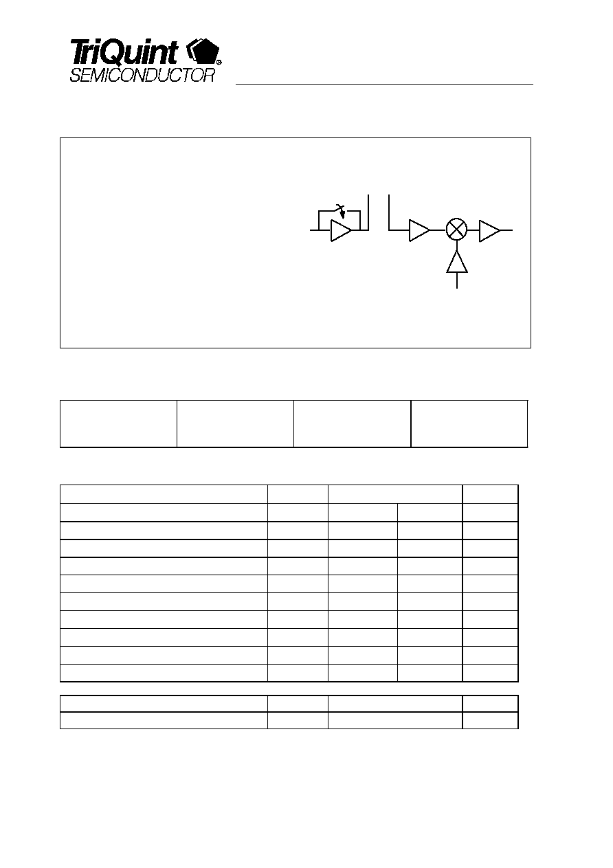
IF Out
LNA
LO
Type
Marking
Ordering code
(tape and reel)
Package
CMH192
H192
Q62705-K608
VQFN-20
Maximum Ratings
Symbol
Value
Unit
min max
Supply Voltage
VDD 0 6 V
DC-Voltage at RF Ports
VRF -
0.3 0.3 V
DC-Voltage at GND Ports
VGND -
0.3 0.3 V
DC-Voltage at CNTL Ports
VCNTL
0
0.3 + VDD V
Power into LO Input
Pin,LO 10 dBm
Power into RF-IF Ports
Pin, RF
10
dBm
Operating Temperature
T
a
-40 85 ∞C
Channel Temperature
TCh 150
∞C
Storage Temperature
Tstg -55 150 ∞C
Thermal Resistance
Channel to Soldering Point (GND)
RthChS 102 ∞C
/W
CMH192 ≠ Datasheet (October 1
st
, 2002)
p
g. 1/11

CMH192 ≠ Datasheet (October 1
st
, 2002)
p
g. 2/11
Electrical Characteristics
Parameter min
typ
RF ≠ Frequency / US
1930
-
1990
MHz
LO ≠ Frequency / US
(1)
1780
-
MHz
RF ≠ Frequency / Korean
1840
-
1870
MHz
LO ≠ Frequency / Korean
(1)
1590
-
1820
MHz
IF Frequency range
50
-
250
MHz
LO Power Input
-7.0
-
0.0
dBm
Supply Voltage (Vdd)
2.7
-
4.0
V
High Logic Level (H)
V
DD
≠ 0.2
-
V
DD
V
Low Logic Level (L)
0.0
-
0.2
V
1) High-side LO is also supported
LNA ≠ Performance of LNA
Test conditions: Ta = 25∞C, VDD= 2.7 V, PRF= -22 dBm, fRF = 1960 MHz, LOW=GND, HIGH=Vdd
Mode ≠ High Gain, High Linearity
min
typ
max
Unit
Operating Current
7
mA
Noise Figure
1.1
dB
Gain
Input / Output return loss
10
dB
3rd Order Input Intercept Point
8.5
dBm
Mode ≠ High Gain, Reduced Current
min
Typ
max
Unit
Operating Current
5
mA
Noise Figure
1.2
dB
Gain
Input / Output return loss
10
dB
3rd Order Input Intercept Point
7.5
dBm
Mode ≠ Low Gain, By-Pass Mode
min
Typ
max
Unit
Operating Current
0
mA
Noise Figure
4.5
dB
Gain
Input / Output return loss
10
dB
3rd Order Input Intercept Point
25
dBm
5
dB
12.3
dB
12.5
dB
1940
GaAs MMIC CMH192
max
Unit

GaAs MMIC CMH192
MIXER - Electrical Characteristics of Mixer section
Test conditions: Ta = 25∞C; VDD= 2.7V, PLO = -7 dBm,PRF=-22 dBm, fRF = 1960 MHz,
f
LO
= f
RF
- f
IF
, fIF = 210MHz, LOW=GND, HIGH=Vdd
Mode ≠ High Linearity
min
typ
max
Unit
Operating Current
15
mA
Conversion Gain
15.0
dB
Noise Figure
3.5
dB
3rd Order Input Intercept Point
5.5
dBm
RF Input return loss
10
dB
LO Input return loss
10
dB
IF Output Impedance
(1)
350
-
j*515
Mode ≠ Reduced Current
min
typ
max
Unit
Operating Current
12
mA
Conversion Gain
14.5
dB
Noise Figure
3.8
dB
3rd Order Input Intercept Point
4
dBm
RF Input return loss
10
dB
LO Input return loss
10
dB
IF Output Impedance
(1)
350
-
j*515
1) IF Output externally tuned to desired impedance
FULL CHAIN ≠ LNA/Downconverter Characteristics
Test conditions: Ta = 25∞C; VDD= 2.7V, PLO = -7 dBm, PRF=-22 dBm, fRF = 1960 MHz,
f
LO
= f
RF
- f
IF
, fIF = 210MHz, LOW=GND, HIGH=Vdd
Mode ≠ High Gain, High Linearity
min
typ
max
Unit
Total operating Current
22.0
mA
Conversion Gain
(1)
24.5
Noise Figure
1.7
dB
Input IP3
-4.5
dBm
LNA Input IP3
10.0
dBm
1) Assumes 3 dB loss for image filter, value is calculated based on gain measurement of LNA and
downconverter
dB
CMH192 ≠ Datasheet (October 1
st
, 2002)
p
g. 3/11

CMH192 ≠ Datasheet (October 1
st
, 2002)
p
g. 4/11
GaAs MMIC CMH192
FULL CHAIN ≠ LNA/Downconverter Characteristics (continued)
Test conditions: Ta = 25∞C; VDD= 2.7V, PLO = -7 dBm, PRF=-22 dBm, fRF = 1960 MHz,
f
LO
= f
RF
- f
IF
, fIF = 210MHz, LOS=GND, HIGH=Vdd
Mode ≠ High Gain, Reduced Current
min typ max
Unit
Total operating Current
17
mA
Conversion Gain
(1)
23.5
Noise Figure
1.8
dB
Input IP3
-5.5
dBm
LNA Input IP3
7.5
dBm
Mode ≠ Low Gain (LNA bypass)
min
Typ
max
Unit
Total operating Current
12
mA
Conversion Gain
(1)
7.2
Noise Figure
11.5
dB
Input IP3
11.5
dBm
1) Assumes 3.0 dB loss for image filter, value is calculated based on gain measurement
of LNA and downconverter
Truth Table
Control
Voltage
Operating Mode
Gain Ctl
Rcv Only
High Gain & Linearity
H
H
High Gain, Low Current
H
L
Low Gain
L
L
dB
dB

GaAs MMIC CMH192
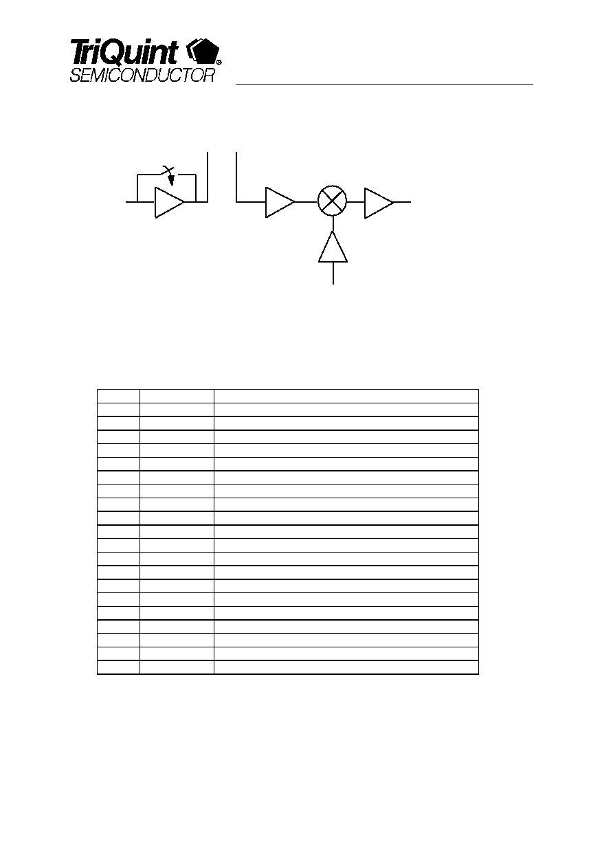
PIN Assignments & Functional Block Diagram
MIXE
RF
IF
LN
LO
Pin Assignments:
Truth Table:
5
I
PIN
Symbol
Description
1
LO in
LO Input
2
GND
Ground
3
LOA Vdd
Supply voltage for LO Buffer Amp
4
Mix Out
Mixer IF Output
F Mtch
IF input match connection
6
IF In
IF amplifier input
7
GND
Ground
8
IFA src
IF Amplifier FET source ground
9
IFA out
IF Amplifier output
10
GND
Ground
11
RFA Vdd
Supply voltage for RFA
12
RFA in
Mixer input from image filter
13
Rcv
Current mode control
14
Vdd
Supply voltage
15
LNA out
RF output of LNA
16
LNA Vdd
Supply voltage for LNA
17
GND
Ground
18
LNA in
RF Input to LNA
19
GND
Ground
20
Gctl
Gain mode control for LNA
CMH192 ≠ Datasheet (October 1
st
, 2002)
p
g. 5/11

GaAs MMIC CMH192
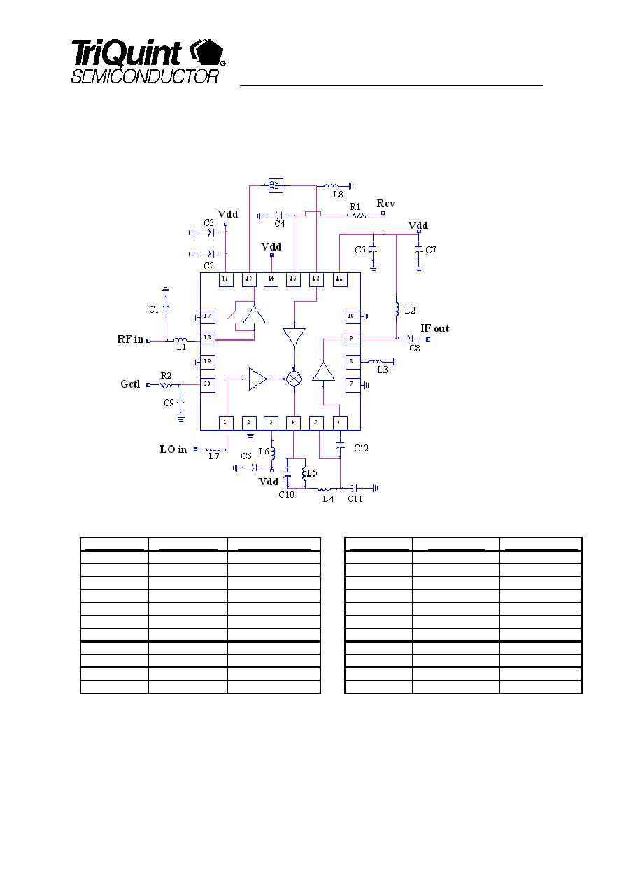
Applications Circuit:
Component
Description
Package Type
Component
Description
Package Type
C1
CAP, 1 pF
0402
C12
CAP, 100 pF
0402
C2
CAP, 22 pF
0402
L1
IND, 5.6 nH
0402
C3
CAP, 10K pF
0402
L2
IND, 120 nH
0603
C4
CAP, 100 pF
0402
L3
IND, 100 nH
0603
C5
CAP, 22 pF
0402
L4
IND, 82 nH
0603
C6
CAP, 1000 pF
0402
L5
IND, 2.7 nH
0402
C7
CAP, 10K pF
0402
L6
IND, 5.6 nH
0402
C8
CAP, 3.3 pF
0402
L7
IND, 5.6 nH
0402
C9
CAP, 100 pF
0402
L8
IND, 12 nH
0402
C10
CAP, 2 pF
0402
R1
RES, 100 KOHM
0402
C11
CAP, 4 pF
0402
R2
RES,100 KOHM
0402
CMH192 ≠ Datasheet (October 1
st
, 2002)
p
g. 6/11

GaAs MMIC CMH192
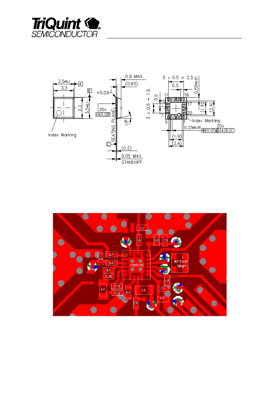
Package Outline ≠ VQFN 20
Recommended PCB Layout:
100pF 0402 SMT capacitor, 3 places
(Murata GRP1555C7H100JZ01 or equivalent )
CMH192 ≠ Datasheet (October 1
st
, 2002)
p
g. 7/11

CMH192 ≠ Datasheet (October 1
st
, 2002)
p
g. 8/11
GaAs MMIC CMH192
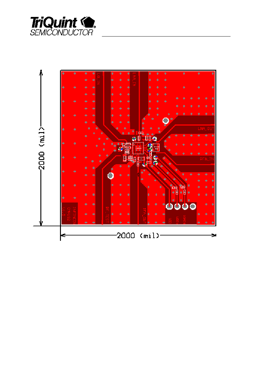
Evaluation Board:

GaAs MMIC CMH192
CMH192 ≠ Application Information
DC Biasing
:
Supply Voltage
One regulated voltage source is needed for CMH192. On the evaluation board it
is labeled VDD.
Minimum LO Power for Proper Biasing
For proper biasing of the CMH192, a minimum LO input power is required. If the
part is turned ON without any LO drive applied all currents will be extremely high.
The minimum LO required is approximately ≠9 dBm. Operation with LO input
powers below the minimum value causes the current to increase in all amplifier
stages. For higher LO input power levels the current stays relatively constant over a
wide range of LO powers. Proper matching of the LO amplifier is also important to
achieve the lowest current consumption and to minimize the required LO input
power.
Adjustable Current Level
The CMH192 can operate in two different current/linearity modes: High Linearity
(with higher current) and Reduced Current (lower linearity). To operate with reduced
current the voltage on pin 13 (RCV) should be set LOW. Some additional current
reduction can be achieved by reducing the voltage at pin 14 by placing a resistor
between VDD and pin 14. The current pulled by pin 14 is approximately 1 mA.
Higher currents can be realized by using a higher VDD voltage.
Tuning LO and IF Amplifiers:
The CMH192 can be tuned to utilize either high or low side LO frequencies and
allows a wide range of IF frequencies. Depending on the chosen frequency plan the
off chip components for the LO and IF amplifiers will need to be optimized. An
application circuit with all component values is provided for low side LO injection with
IF frequency of 210 MHz (RF freq 1930 ≠ 1960 MHz)
Two external components (L6 and L7) are required for tuning the LO. L6 is
critical for setting the minimum current and to achieve the constant DC current over
the operating band. L7 sets the LO input match.
Components L4, C9 and C11 form the input match for the IF amplifiers and will
vary depending on the chosen IF frequency. The inductor on pin 8 allows
adjustment to the gain of the IF amplifier.
Output matching components shown in the application circuit provide a
transformation for a 50 Ohm load impedance. The output impedance for the IFA
(looking into pin 9) at 210 MHz is approximately (350 - j*515) Ohms.
CMH192 ≠ Datasheet (October 1
st
, 2002)
p
g. 9/11

GaAs MMIC CMH192
Downconverter Gain Adjustment:
The Downconverter gain can be adjusted by changing the source feedback
inductor L3 for the IFA. Higher inductance will give lower downconverter gain and
typically improve the IIP3.
Gain/Current Control Pins:
LOW = 0 to 0.2 V
HIGH = Vdd to (Vdd ≠ 0.2) V
VGAIN ≠ select between high and low gain states in the LNA.
VGAIN = HIGH: LNA ON (~12 dB Gain, ~ 6.5 mA current)
VGAIN = LOW: LNA bypassed (~ 4 dB Loss, no current)
VRCV - selects Current/Linearity mode (changes current in LNA/RFA/IFA)
VRCV = LOW selects Reduced Current Mode
VRCV = HIGH selects High Linearity Mode.
Other Notes:
Inductor L1 is critical for setting the Noise Figure of the LNA. A high Q wire wound
inductor (e.g. Coilcraft) is recommended to achieve minimum NF.
Inductor L5 and Capacitor C10 form a "tank circuit" to terminate the RF in the mixer.
These components should be placed in parallel close to pin 4. These elements may
require tuning depending on component vendor and board parasitics to achieve flat
conversion gain vs. frequency.
Inductor L8 is necessary for proper operation of the circuit for ESD protection.
Lower RF frequencies (i.e. Korean PCS or GPS) may be accommodated by adding
inductance between the LNA and RFA VDD pins and their bypass capacitors.
LNA current can be determined by subtracting the current in Low Gain mode from
the current in High Gain mode (keeping VRCV and VMODE constant).
Control lines (G_CNTL, VRCV and VMODE) have an input impedance of greater
than 1 M
when Vdd is ON. When VDD is off, they have approximately 20 K input
impedance.
CMH192 ≠ Datasheet (October 1
st
, 2002)
p
g. 10/11

Published by TriQuint Semiconductor GmbH, Marketing, Konrad-Zuse-Platz 1, D-81829
Munich.
Copyright TriQuint Semiconductor GmbH 2002. All Rights Reserved.
As far as patents or other rights of third parties are concerned, liability is only assumed for
components per se, not for applications, processes and circuits implemented within
components or assemblies.
The information describes the type of component and shall not be considered as assured
characteristics.
Terms of delivery and rights to change design reserved.
For questions on technology, delivery, and prices please contact the Offices of TriQuint
Semiconductor in Germany or the TriQuint Semiconductor Companies and Representatives
worldwide.
Due to technical requirements components may contain dangerous substances. For information
on the type in question please contact your nearest TriQuint Semiconductors Office.
pg.
11/11
GaAs MMIC CMH192
