 | –≠–ª–µ–∫—Ç—Ä–æ–Ω–Ω—ã–π –∫–æ–º–ø–æ–Ω–µ–Ω—Ç: CMY212 | –°–∫–∞—á–∞—Ç—å:  PDF PDF  ZIP ZIP |

For additional information and latest specifications, see our website:
www.triquint.com
2
Revision B, December 14, 2005
2
Mixer
LO in
GND
IF amp
in
Mixer
V
DD
CMY212
GND
Mixer
RF in
IF out
IF amp
out
IF amp
Source
1
8
6
7
5
4
3
Features
∑
Typical overall performance at cellular
frequencies (for P
LO
= -4dBm operation
conditions: 3V, 11 mA; f
RF
= 881 MHz;
f
LO
= 966 MHz):
o
Gain 10 dB
o
Input IP3 9 dBm
o
Noise figure 8 dB
∑
RF-frequency range 0.5 - 2.5 GHz
∑
Operating voltage range: 2.6 to 5V
∑
Small SCT598 plastic package
CMY212
Datasheet
Ultra-linear Mixer with Integrated IF Amp and LO Buffer
Description
CMY212 is a general purpose down-converter
device designed for multiple applications such
as cellular and PCS mobile phones, ISM
bands, GPS receivers, L-band satellite
terminals, WLAN and pagers. Due to its
excellent intermodulation characteristics and
its high conversion gain, CMY212 is
particularly suited for CDMA receiver
applications.
The device combines an ultra-linear mixer
with LO - driver and a single stage IF-amplifier
in a very small SCT598 package. The mixer
section of CMY212 combines low conversion
losses and excellent intermodulation
characteristics with low requirements of LO -
and DC-power. The internal level controlled
LO-Buffer enables a good performance over a
wide LO level range. The input and output
matching of the IF amplifier can be adapted
externally within a frequency range from 45 to
250 MHz.
Applications
∑
Down Converter for
Multiple Wireless
Applications
∑
Cellular and PCS
Mobile Phones
∑
Particularly Suited for
CDMA Receivers
∑
ISM and WLAN
Receivers
∑
GPS Receivers
Package Outline and Pin
Configuration,
SCT598

CMY212 Datasheet
For additional information and latest specifications, see our website:
www.triquint.com
3
Revision B, December 14, 2005
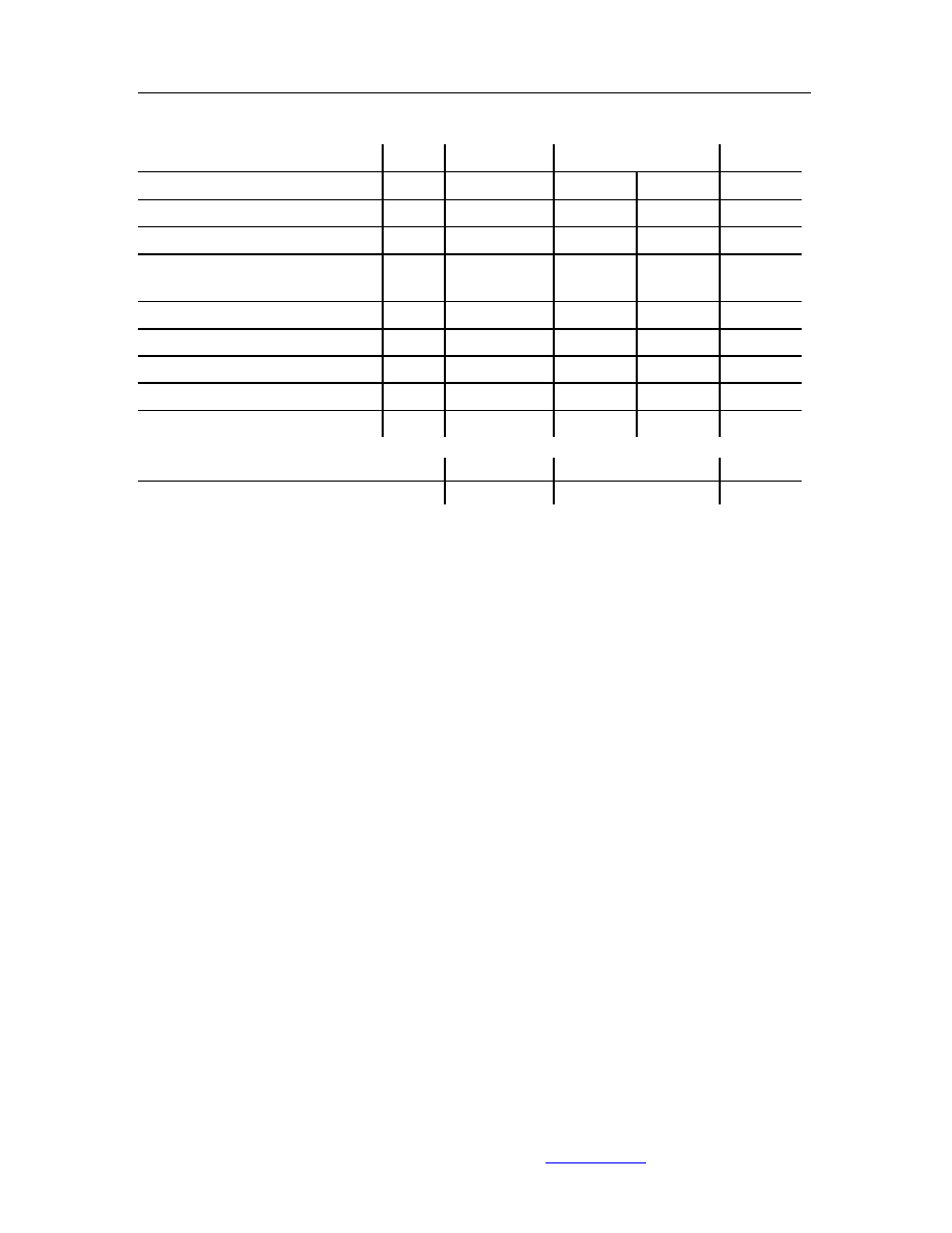
Maximum Ratings
Parameter Port
Symbol
Value
Unit
min max
Supply Voltage
3,6
V
DD
0 5 V
DC-Voltage at LO Input
4
V
6
-3
0,5
V
DC-Voltage at
Mixer RF-IF Port
1 V
8
- 0,5
+ 0,5
V
Power into Mixer RF Port
1
P
RF
10
dBm
Power into LO Input
4
P
in,LO
-10 10 dBm
Channel Temperature
T
Ch
150
∞C
Operating Temperature
T
op
-30
85 ∞C
Storage Temperature
T
stg
-55
150
∞C
Thermal Resistance*
Channel to Soldering Point (GND)
R
thChS
260 K/W

CMY212 Datasheet
For additional information and latest specifications, see our website:
www.triquint.com
4
Revision B, December 14, 2005
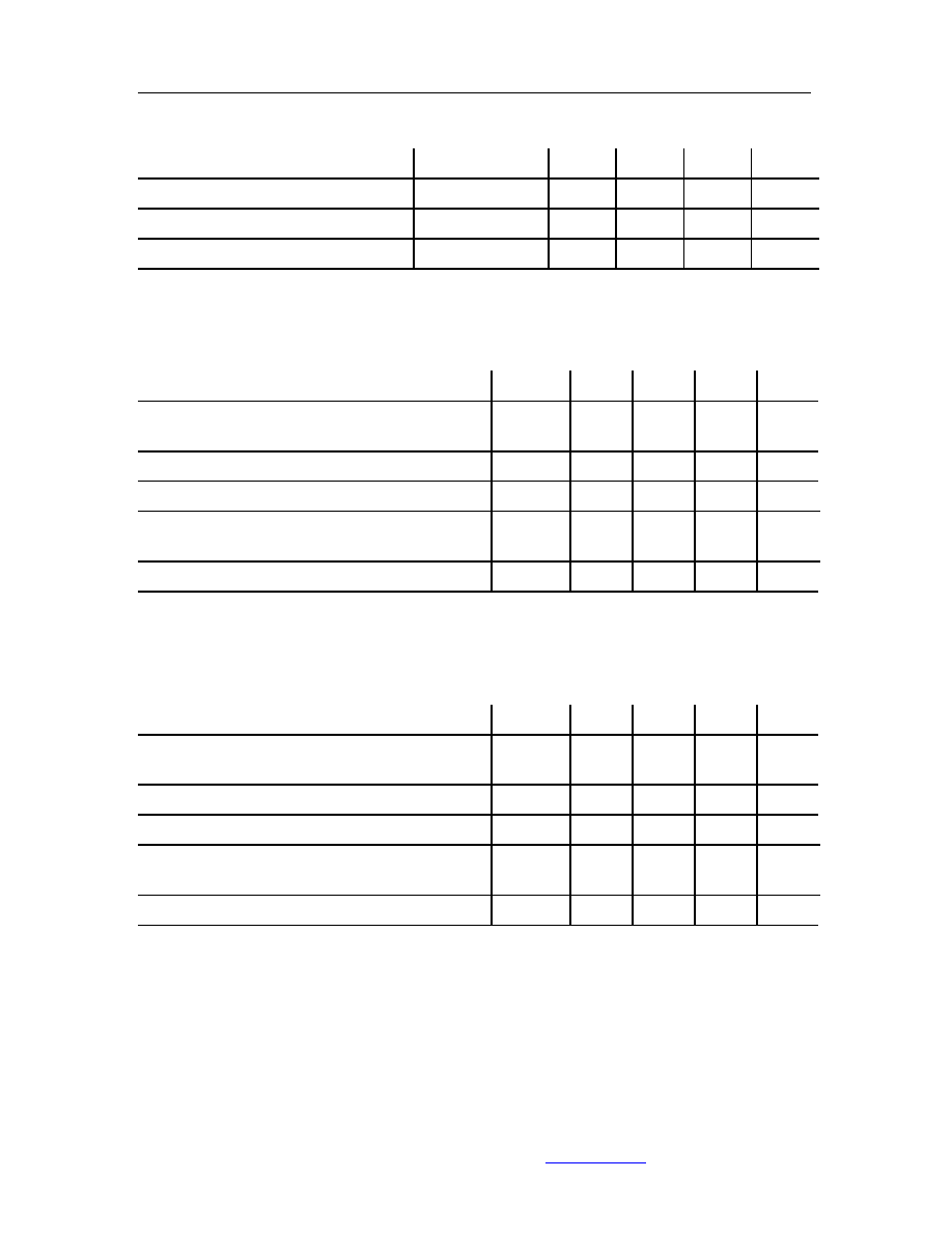
Electrical Characteristics
Parameter, Comment
min
typ
max
Unit
RF - frequency range
external match
0.5
-
2.5
GHz
LO - Frequency range
external match
0.5
-
2.5
GHz
IF Frequency range
external match
45
250
MHz
Typical performance at cellular frequencies*:
Ta = 25∞C; VDD= 3V, fRF = 881MHz; fLO = 966MHz; PLO = -4dBm; fIF = 85MHz,
Z
S
= Z
L
= 50 Ohm; unless otherwise specified
Parameter, Test Conditions
Symbol
Min
typ
max
Unit
Total operating Current (Mixer + IF
amplifier)
I
op
- 11 - mA
Conversion Gain
G
c
- 10 - dB
SSB Noise Figure
F
ssb
- 8 - dB
RF Input -/ IF Output return loss
(external matching required)
RFIrl /
IFOrl
- 10 - dB
3rd Order Input Intercept Point
IIP3
-
10
-
dBm
Test conditions at PCS frequencies:
Ta = 25∞C; VDD= 3V, fRF = 1960MHz; fLO = 1750MHz; PLO = -4dBm; fIF = 210MHz,
Z
S
= Z
L
= 50 Ohm; unless otherwise specified
Parameter, Test Conditions
Symbol
Min
Typ
max
Unit
Total operating Current
(Mixer + IF amplifier)
I
op
-
12
14
mA
Conversion Gain
G
c
8.5
9.5
-
dB
SSB Noise Figure
F
ssb
- 8.5 - dB
RF Input -/ IF output return loss
(external matching required)
RFIrl /
IFOrl
- 10 - dB
3rd Order Input Intercept Point
IIP3
10
11.5
-
dBm
* IMPORTANT NOTE:
During production, the RF performance at PCS frequencies is screened. The passed devices also
achieve the specified RF performance at cellular frequencies.

CMY212 Datasheet
For additional information and latest specifications, see our website:
www.triquint.com
5
Revision B, December 14, 2005
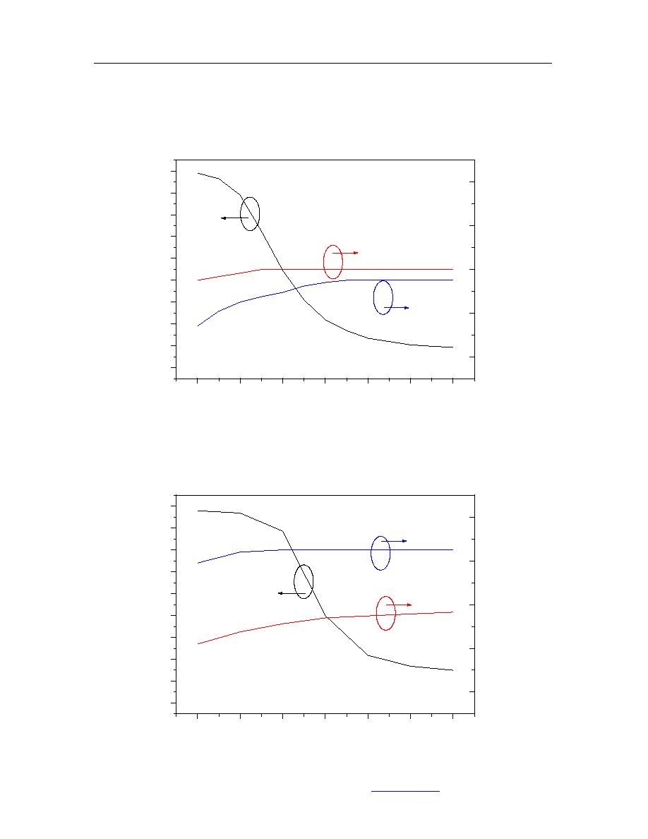
Electrical Characteristics (cont)
Typical device behavior at cellular frequencies:
Ta = 25∞C; VDD= 3V, fRF = 881MHz; fLO = 966MHz; fIF = 85MHz;
Z
S
= Z
L
= 50 Ohm; unless otherwise specified
-12
-10
-8
-6
-4
-2
0
8
10
12
14
16
18
20
22
24
26
I
op
IIP3
Gain
O
p
e
r
at
i
ng C
u
r
r
e
nt
[
m
A
]
LO Power [dbm]
6
8
10
12
14
G
a
i
n
[d
B
], IIP
3
[d
B
m
]
Typical device behavior at PCS frequencies:
Ta = 25∞C; VDD= 3V, fRF = 1960MHz; fLO = 1750MHz; fIF = 210MHz;
Z
S
= Z
L
= 50 Ohm; unless otherwise specified
-12
-10
-8
-6
-4
-2
0
8
10
12
14
16
18
20
22
24
26
I
op
IIP3
Gain
O
per
a
t
i
n
g
C
u
r
r
ent
[
m
A
]
LO Power [dbm]
6
8
10
12
14
G
a
i
n
[d
B
], I
I
P
3
[d
B
m
]

CMY212 Datasheet
For additional information and latest specifications, see our website:
www.triquint.com
6
Revision B, December 14, 2005
Applications Information
Test Circuit:
CMY212 Functional
Block Diagram
RF
Input
IF Output
1
2
3
4
8
6
5
7
+3V
LO
Input
GND
Vs Cap
LO
Input
VD
IF
B
u
ff
e
r
Mi
x
e
r
IF Input
RF
Input
+3V
IF
Output
Cext4
Lext4
Lext5
Cext5
Lext1
Cext1
Lext2
Cext2
Lext3
Cext3
Cext6
Cext8
GND
Cext7
External components for cellular frequencies
f
RF
= 875MHz; f
LO
= 960MHz; f
IF
= 85MHz
Capacitors
(Murata 0402)
Inductors
(Toko)
Cext1 2
pF
Lext1
18
nH
LL1005
Cext2
1 nF
Lext2
270 nH
LL1608
Cext3 20
pF
Lext3
220
nH
LL1608
Cext4 100
pF
Lext4
12
nH
LL1005
Cext5 1
nF
Lext5
15
nH
LL1005
Cext6 1
nF
Cext7 3.3
pF
Cext8 100
nF
Lext8
22
nH
LL1005
External components for PCS frequencies
f
RF
= 1960MHz; f
LO
= 1750MHz; f
IF
= 210MHz
Capacitors
(Murata 0402)
Inductors
(Toko)
Cext1 1
pF
Lext1
5.6
nH
LL1005
Cext2 1
nF
Lext2
68
nH
LL1608
Cext3 8
pF
Lext3
68
nH
LL1608
Cext4 22
pF
Lext4
4.7
nH
LL1005
Cext5 1
nF
Lext5
4.7
nH
LL1005
Cext6 1
nF
Cext7 3
pF
Cext8 100
nF

CMY212 Datasheet
For additional information and latest specifications, see our website:
www.triquint.com
7
Revision B, December 14, 2005
Applications Information (cont)
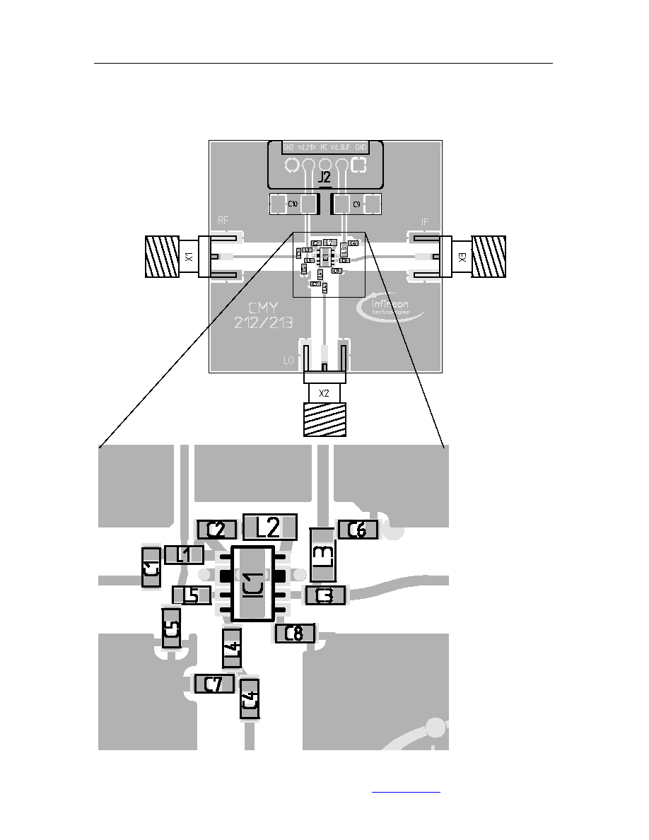
PCB Layout:
Size: 35 x 35 mm≤
RF
Input
LO
Input
IF
Output

CMY212 Datasheet
For additional information and latest specifications, see our website:
www.triquint.com
8
Revision B, December 14, 2005
General description and notes
CMY212 is a general purpose down-converter device designed for multiple applications such as
cellular and PCS mobile phones, ISM bands, GPS receivers, L-band satellite terminals, WLAN and
pagers. Due to its excellent intermodulation characteristics and its high conversion gain, CMY212 is
particularly suited for CDMA receiver applications.
The device combines an ultra-linear mixer with LO - driver and a single stage IF-amplifier in a very
small SCT598 package. The mixer section of CMY212 combines low conversion losses and excellent
intermodulation characteristics with low requirements of LO - and DC-power. The internal level
controlled LO-Buffer enables a good performance over a wide LO level range. The input and output
matching of the IF amplifier can be adapted externally within a frequency range from 45 to 250 MHz.
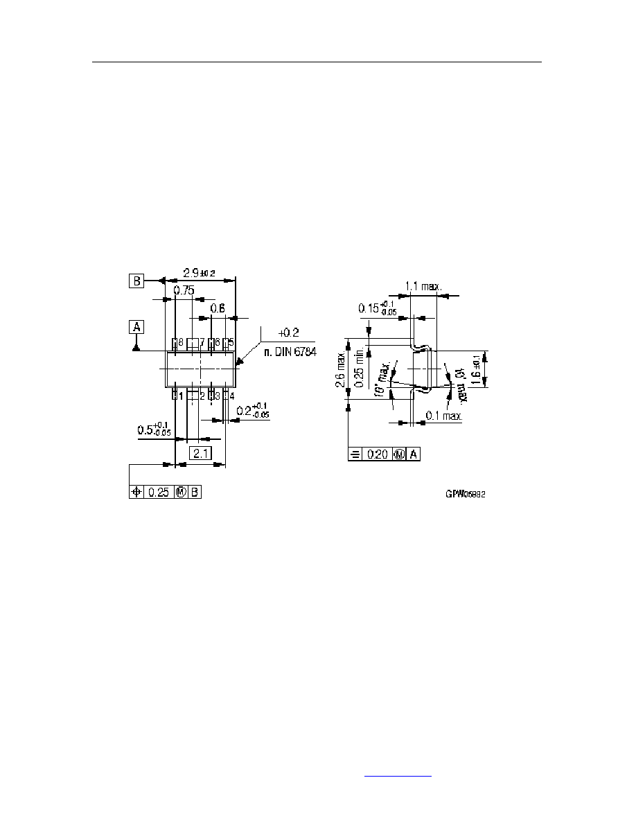
Semiconductor Device Outline SCT598-8-1

CMY212 Datasheet
For additional information and latest specifications, see our website:
www.triquint.com
9
Revision B, December 14, 2005
Ordering Information
Type
Marking
Ordering code
(tape and reel)
Package
1)
CMY212
M5s
Q62702-M0026
SCT598-8-1
Additional Information
This part is
compliant with RoHS directive (Restrictions on the Use of Certain Hazardous Substances
in Electrical and Electronic Equipment).
The part is rated Moisture Sensitivity Level 1
at 260∞C per JEDEC standard IPC/JEDEC J-STD-020.
ESD: Electrostatic discharge sensitive device. Observe handling Precautions.
For latest specifications, additional product information, worldwide sales and distribution locations, and information
about TriQuint:
Web:
www.triquint.com
Tel: (503) 615-9000
Email:
info_wireless@tqs.com
Fax: (503) 615-8902
For technical questions and additional information on specific applications:
Email:
info_wireless@tqs.com
The information provided herein is believed to be reliable; TriQuint assumes no liability for inaccuracies or
omissions. TriQuint assumes no responsibility for the use of this information, and all such information shall be
entirely at the user's own risk. Prices and specifications are subject to change without notice. No patent rights or
licenses to any of the circuits described herein are implied or granted to any third party.
TriQuint does not authorize or warrant any TriQuint product for use in life-support devices and/or systems.
Copyright © 2005 TriQuint Semiconductor, Inc. All rights reserved
.

