 | ÐлекÑÑоннÑй компоненÑ: CSH210 | СкаÑаÑÑ:  PDF PDF  ZIP ZIP |
Datenblatt CMY210a; großsignalmischer 500MHz bis 2GHz

CSH210
Datasheet
Features:
· TX-RX Diversity Switch for mobile
communications:
o Insertion Loss: 0.4 dB
o Isolation: 20 dB
o VSWR: 1.3:1
o P-0.1dB: +26 dBm
· RF-frequency range DC - 3 GHz
· No supply voltage
· Positive control voltage
· Small SOT363 plastic package
TX-RX Diversity Switch
Description:
CSH210 is a general purpose single-pole,
single-throw switch device designed for
mobile communications applications such as
cellular and PCS mobile phones, ISM bands,
GPS receivers, L-band satellite terminals,
WLAN and pagers. The device is based on
pHEMT technology and exhibits very low
insertion loss and high intermodulation
performance.
The CSH210 does not need a supply voltage
and switching is accomplished with a positive
control voltage. The device exhibits excellent
VSWRs and isolation as well. It is useable
from DC to 3 GHz.
Applications:
·
Antenna Diversity
Switching
· TX-RX Switching
· Mobile Phones
·
ISM and WLAN
·
L-Band Satellite
Terminals
Package Outline:
SOT363
Pin configuration:
1: RF
Port
2: GND
3: RF
Port
4: Control
V2
5: RF
Common
6: Control
V1
For further information, please visit
www.triquint.com
pg.
1/7
May 1st, 2003

CSH210 Datasheet
Electrical Performance:
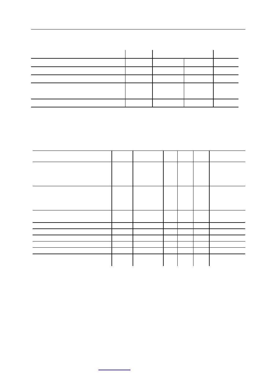
Maximum Ratings
Symbol
Value
Unit
min
max
Control Voltage Range
Vcntrl
-5
5
V
RF Input Power
Pin
3
W
Junction Temperature
@ 30dbm input and 25°C
Tj
50
°C
Storage Temperature
Tstg
-55
150
°C
Electrical Characteristics:
(T=25C; Vcntrl=3.0V; Pin=0dBm)
Parameter Symbol
Test
Condition
min typ max
Unit
Insertion Loss RFC-RF1, RFC-RF2
ILRF DC-0.5GHz
DC-1.0GHz
DC-2.0GHz
DC-3.0GHz
0.25
0.3
0.4
0.5
0.3
0.4
0.6
0.75
dB
Isolation RF1-RF2
ISOL DC-0.5GHz
DC-1.0GHz
DC-2.0GHz
DC-3.0GHz
25
22
18
15
28
24
20
18
dB
VSW R* (all ports)
VSW R
DC-2.5GHz
DC-3.0GHz
1.3:1
1.5:1
Gate Leakage
IL
0.1
mA
Trise /Tfall (10% RF to 90%RF)
10
nS
Ton /Toff (50% CNTRL -90%/10%RF)
20
nS
Output Power for 0.1 dB compression
P-0.1
DC-3.0GHz
26
dBm
Output Power for 1 dB compression
P1
DC-3.0GHz
30
dBm
Intermodulation Intercept Point
IP3
Pin=25dBm
Freq.=1.0Ghz
50 56
dBm
*VSWR defined for Insertion Loss State Only
For further information, please visit
www.triquint.com
pg.
2/7
May 1st, 2003

CSH210 Datasheet
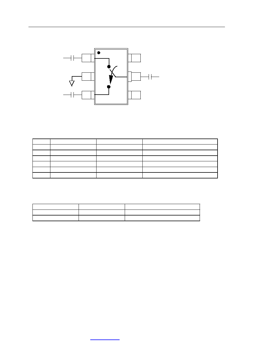
PIN Assignments & Functional Block Diagram
1
2
3
6
4
5
V1
V2
RFC
RF1
RF2
GND
*External DC blocking capacitor required 100pF 3 places
Pin Assignments:
Truth Table:
PIN
Symbol
Abbreviation
Description
1
RF OUTPUT 1
RF1
RF OUTPUT
2
GND
GND
Circuit common and DC return
3
RF OUTPUT 2
RF2
RF OUTPUT
4
V_CONTROL 2
V2
RF OUTPUT 2 control
5
RF COMMON
RFC
Common RF port
6
V_CONTROL 1
V1
RF OUTPUT 1 control
V1
V2
Through Path
3V
0V
RFC RF1
0V
3V
RFC RF2
For further information, please visit
www.triquint.com
pg.
3/7
May 1st, 2003

CSH210 Datasheet
For further information, please visit
www.triquint.com
Electrical Performance, Continued:
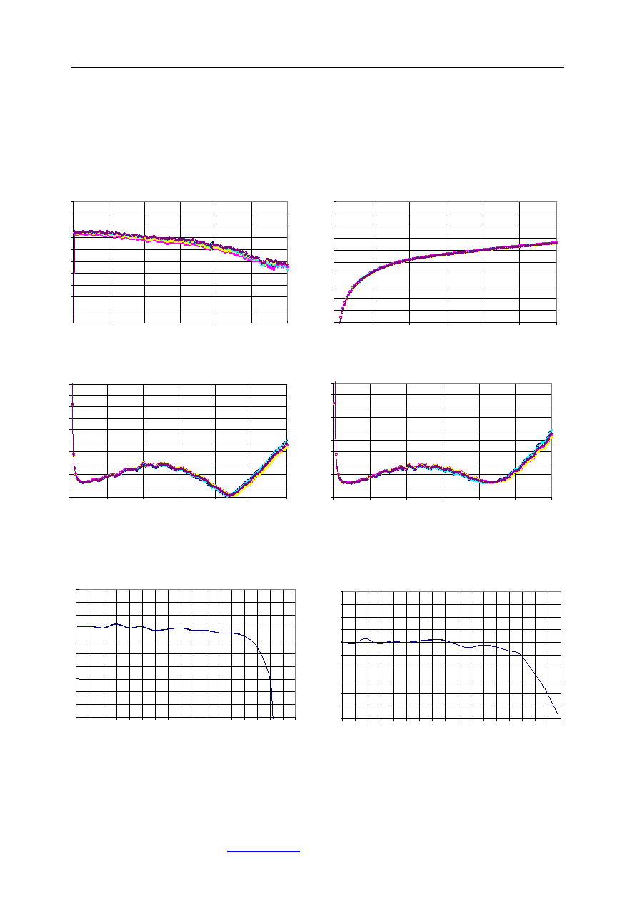
Measured Results:
(All Ports connected to 50ohms, Pin=0dBm, Vcntrl=3V unless otherwise specified)
Insertion Loss vs. Frequency
-1
-0.9
-0.8
-0.7
-0.6
-0.5
-0.4
-0.3
-0.2
-0.1
0
0.00
0.50
1.00
1.50
2.00
2.50
3.00
Frequency (GHz)
Insertion L
o
ss (dB
)
Isolation vs. Frequency
-50
-45
-40
-35
-30
-25
-20
-15
-10
-5
0
0.00
0.50
1.00
1.50
2.00
2.50
3.00
Frequency (GHz)
Isolation (d
B)
Input VSWR vs. Frequency
1
1.1
1.2
1.3
1.4
1.5
1.6
1.7
1.8
1.9
2
0.00
0.50
1.00
1.50
2.00
2.50
3.00
Frequency (GHz)
VSW
R
Output VSWR vs. Frequency
1
1.1
1.2
1.3
1.4
1.5
1.6
1.7
1.8
1.9
2
0.00
0.50
1.00
1.50
2.00
2.50
3.00
Frequency (GHz)
VS
WR
pg.
4/7
May 1st, 2003
Insertion Loss vs. Input Power at F=1GHz
(RFC - RF1, RFC - RF2)
-1
-0.9
-0.8
-0.7
-0.6
-0.5
-0.4
-0.3
-0.2
-0.1
0
15
16
17
18
19
20
21
22
23
24
25
26
27
28
29
30
31
32
Input Power (dBm)
Ins
e
r
t
i
on Loss
(
d
B
)
Insertion Loss vs. Input Power at F=2GHz
RFC - RF1, RFC - RF2
-1
-0.9
-0.8
-0.7
-0.6
-0.5
-0.4
-0.3
-0.2
-0.1
0
15
16
17
18
19
20
21
22
23
24
25
26
27
28
29
30
31
32
Input Power (dBm)
Insertion Loss
(dB
)

CSH210 Datasheet
Electrical Performance, Continued:
Applications Information:
Insertion Loss vs Input Power and Vcntrl
at F=1GHz
-1
-0.9
-0.8
-0.7
-0.6
-0.5
-0.4
-0.3
-0.2
-0.1
0
15
16
17
18
19
20
21
22
23
24
25
26
27
28
29
30
31
32
Input Power (dBm)
In
ser
tio
nLo
ss (dB
)
csh210_1_3.0V/0.0V
csh210_1_3.0V/0.2V
csh210_1_3.0V/0.4V
csh210_1_3.0V/0.6V
csh210_1_2.7V/0.0V
Control Current vs Input Power and Vcntrl
At F=1GHz
0
20
40
60
80
100
120
140
160
15 16 17 18 19 20 21 22 23 24 25 26 27 28 29 30 31 32
Input Power (dBm)
C
ontr
o
l C
u
rre
nt (u
A)
3V / 0.0V
3V / 0.2V
3V / 0.4V
3V / 0.6V
3V / 0.8V
2.7V / 0.0V
Measured Results:
(All Ports connected to 50ohms, Pin=0dBm, Vcntrl=3V unless otherwise specified)
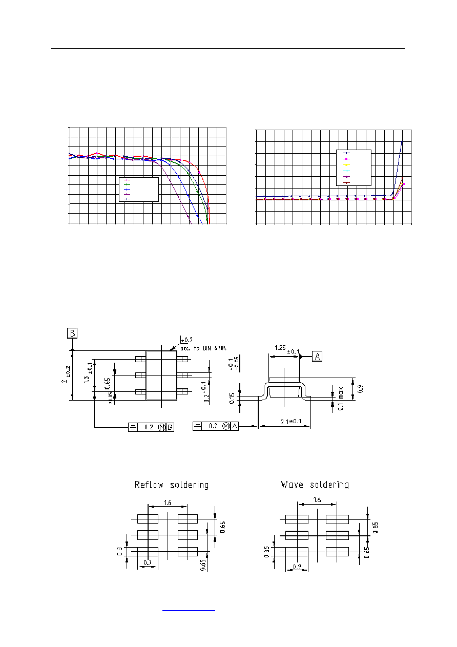
Package Outline - SOT363
Recommended SOT363 Solder Footprint
For further information, please visit
www.triquint.com
pg.
5/7
May 1st, 2003
