 | –≠–ª–µ–∫—Ç—Ä–æ–Ω–Ω—ã–π –∫–æ–º–ø–æ–Ω–µ–Ω—Ç: GA1085 | –°–∫–∞—á–∞—Ç—å:  PDF PDF  ZIP ZIP |
T
R
I Q
U
I
N
T
S E M I C O N D U C T O R , I N C .
SYSTEMS TIMING
SYSTEM TIMING
PRODUCTS
1
For additional information and latest specifications, see our website: www.triquint.com
GA1085
11-Output
Configurable
Clock Buffer
Features
∑ Wide frequency range:
24 MHz to 105 MHz
∑ Output configurations:
Four outputs at f
REF
Four outputs at f
REF
/2
Two outputs at f
REF
/2
with adjustable phase
or
Five outputs at 2x f
REF
Three outputs at f
REF
Two outputs at f
REF
with adjustable phase
∑ Selectable Phase Shift: ≠2t, ≠t,
+t, and +2t (t = 1/f
VCO
)
∑ Low output-to-output skew: 150
ps (max) within a group
∑ Near-zero propagation delay:
≠350 ps +1000 ps (max)
∑ TTL-compatible with 30 mA
output drive
∑ 28-pin J-lead surface-mount
package
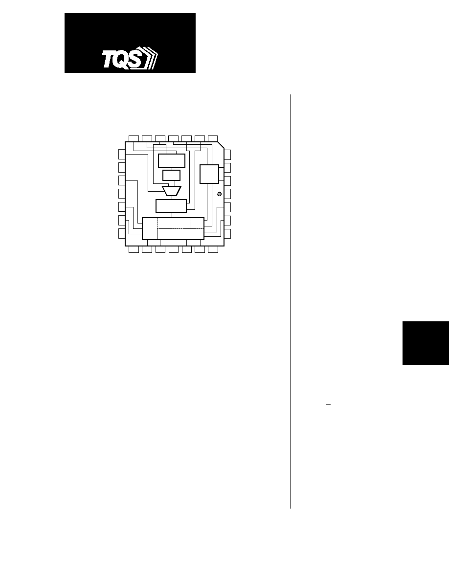
Figure 1. Block Diagram
Output Buffers
VCO
Phase
Detector
VDD
Q10
Q9
GND
Q8
Q7
VDD
TEST
VDD
Q0
GND
Q1
Q2
VDD
FBIN S1 REFCLK S0 F1 F0 GND
GND Q3 Q4 VDD Q5 Q6 GND
1
2
14
13
12
11
10
9
8
7
6
5
4
3
22
21
20
19
18
17
16
15
27
28
25
24
23
26
Phase
Select
MUX
Divide Logic
˜4, ˜5, or ˜6
Group
B
Group A
Group
C
TriQuint's GA1085 is a configurable clock buffer which generates 11 outputs
and operates over a wide range of frequencies--from 24 MHz to 105 MHz.
The outputs are available at either 1x and 2x or at 1x and
1
/
2
x the reference
clock frequency, f
REF
. When one of the Group A outputs (Q4≠Q8) is used as
feedback to the PLL, all Group A outputs will be at f
REF
, and all Group B
(Q0≠Q3) and Group C (Q9, Q10) outputs will be at
1
/
2
x f
REF
. When one of
the Group B outputs is used as feedback to the PLL, all Group A outputs
will be at 2x
REF
and all Group B and Group C outputs will be at f
REF
. The
Shift Select pins select the phase shift (≠2t, ≠t, +t or +2t) for Group C
outputs (Q9, Q10) with respect to REFCLK. The phase shift increment (t)
is equivalent to the VCO's period (1/f
VCO
).
A very stable internal Phase-Locked Loop (PLL) provides low-jitter operation.
This completely self-contained PLL requires no external capacitors or resistors.
The PLL's Voltage-Controlled Oscillator (VCO) has a frequency range from
280 MHz to 420 MHz. By feeding back one of the output clocks to FBIN,
the PLL continuously maintains frequency and phase synchron-ization
between the reference clock (REFCLK) and each of the outputs.
TriQuint's patented output buffer design delivers a very low output-to-output
skew of 150 ps (max). The GA1085's symmetrical TTL outputs are capable
of sourcing and sinking 30 mA.

GA1085
For additional information and latest specifications, see our website: www.triquint.com
2
Functional Description
The core of the GA1085 is a Phase-Locked Loop (PLL)
that continuously compares the reference clock (REFCLK)
to the feedback clock (FBIN), maintaining a zero
frequency difference between the two. Since one of the
outputs (Q0≠Q8) is always connected to FBIN, the PLL
keeps the propagation delay between the outputs and
the reference clock within ≠350 ps +1000 ps.
The internal Voltage-Controlled Oscillator (VCO) has an
operating range of 280 MHz to 420 MHz. The
combination of the VCO and the Divide Logic enables
the GA1085 to operate between 24 MHz and 105 MHz.
The device features six divide modes:
˜
4,
˜
5,
˜
6,
˜
8,
˜
10, and
˜
12. The Frequency Select pins, F0 and F1,
and the output used as feedback to FBIN set the divide
mode as shown in Table 1.
The Shift Select pins, S0 and S1, control the phase
shift of Q9 and Q10 relative to the other outputs. The
user can select from four incremental phase shifts as
shown in Table 2.
The phase-shift increment (t) is calculated using the
following equation:
where
n
is the divide mode.
In the test mode, the PLL is bypassed and REFCLK is
connected directly to the Divide Logic block via the
MUX, as shown in Figure 1. This mode is useful for
debug and test purposes. The various test modes are
outlined in Table 3. In the test mode, the frequency of
the reference clock is divided by 4, 5, or 6.
The maximum rise and fall time at the output pins is
1.4 ns. All outputs of the GA1085 are TTL-compatible
with 30 mA symmetric drive and a minimum V
OH
of 2.4 V.
Power-Up/Reset Synchronization
After power-up or reset, the PLL requires time before it
achieves synchronization lock. The maximum time
required for synchronization (TSYNC) is 500 ms.
Table 1. Frequency Mode Selection
Feedback: Any Group B Output (Q0 ≠ Q3)
Select Pins
Reference Clock
Output Frequency Range
Test
F0
F1
Mode
Frequency Range
Group A: Q4≠Q8
B: Q0≠Q3, C: Q9≠Q10
0
1
0
˜
4
70 MHz ≠ 105 MHz
70 MHz ≠ 105 MHz
35 MHz ≠ 52 MHz
0
0
0
˜
5
56 MHz ≠ 84 MHz
56 MHz ≠ 84 MHz
1
28 MHz ≠ 42 MHz
0
0
1
˜
6
48 MHz ≠ 70 MHz
48 MHz ≠ 70 MHz
24 MHz ≠ 35 MHz
0
1
1
Not Used
N.A.
N.A.
N.A.
Feedback: Any Group A Output (Q4 ≠ Q8)
Select Pins
Reference Clock
Output Frequency Range
Test
F0
F1
Mode
Frequency Range
Group A: Q4≠Q8
B: Q0≠Q3, C: Q9≠Q10
0
1
0
˜
8
35 MHz ≠ 52 MHz
70 MHz ≠ 105 MHz
35 MHz ≠ 52 MHz
0
0
0
˜
10
28 MHz ≠ 42 MHz
56 MHz ≠ 84 MHz
1
28 MHz ≠ 42 MHz
0
0
1
˜
12
24 MHz ≠ 35 MHz
48 MHz ≠ 70 MHz
24 MHz ≠ 35 MHz
0
1
1
Not Used
N.A.
N.A.
N.A.
t =
1
(f
) (n)
REF
Note:
1. This mode produces outputs with 40/60 duty cycle for Q4 ≠ Q8 only.
GA1085
SYSTEM TIMING
SYSTEM TIMING
PRODUCTS
3
For additional information and latest specifications, see our website: www.triquint.com
S0
S1
Phase Difference (Q9, Q10)
0
0
+2t
0
1
+t
1
0
≠t
1
1
≠2t
Table 2. Phase Shift Selection
Table 3. Test Mode Selection
Group A:
Groups B, C:
Test
F0
F1
Mode
Ref. Clock
Outputs Q4≠Q8
Q0≠Q3, Q9, Q10
1
1
0
˜
4
f
REF
f
REF
˜
4
f
REF
˜
8
1
0
0
˜
5
f
REF
f
REF
˜
5
f
REF
˜
10
1
0
1
˜
6
f
REF
f
REF
˜
6
f
REF
˜
12
1
1
1
--
--
--
--
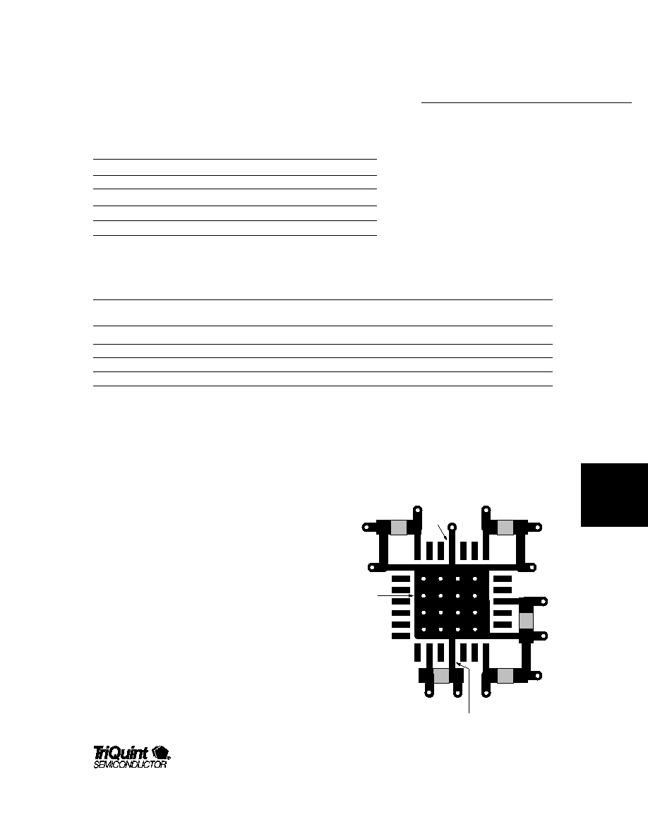
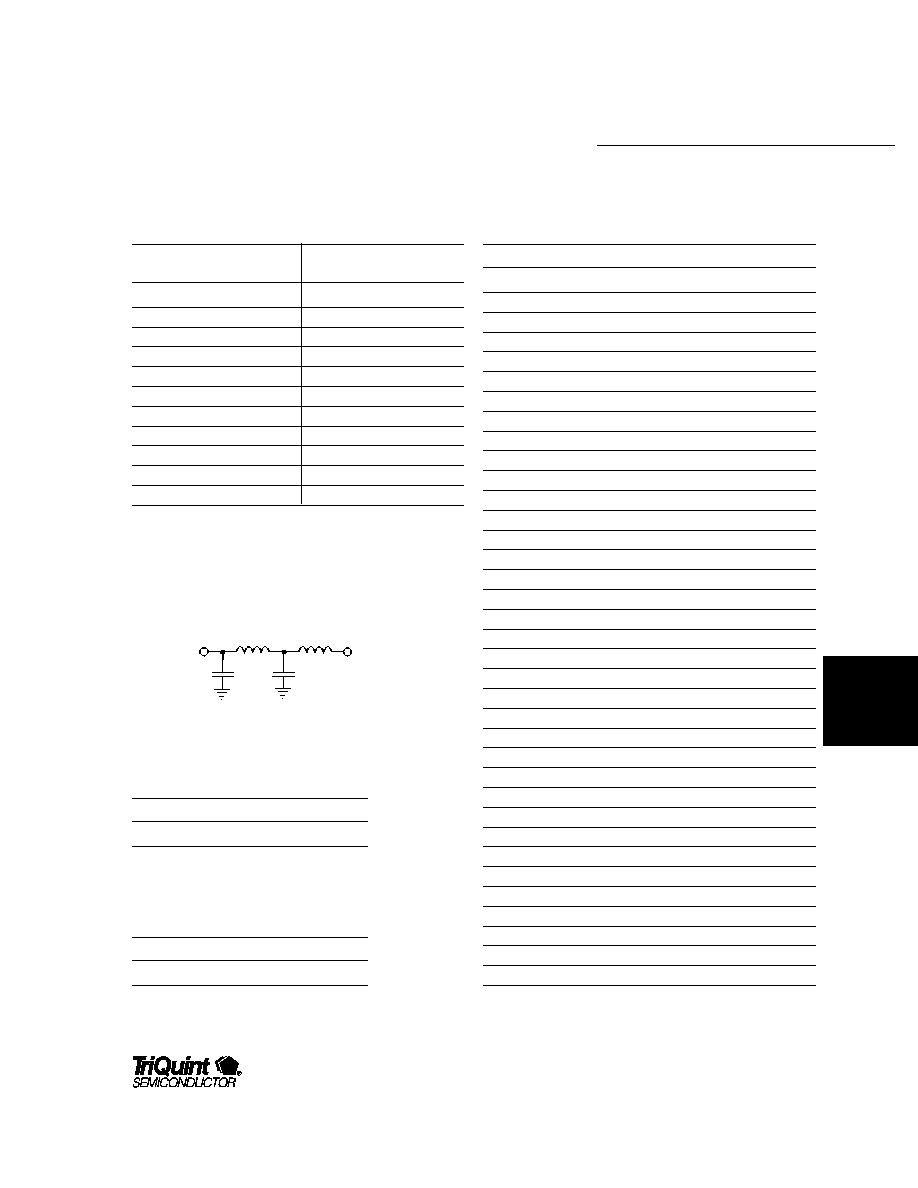
Layout Guidelines
Multiple ground and power pins on the GA1085 reduce
ground bounce. Good layout techniques, however, are
necessary to guarantee proper operation and to meet
the specifications across the full operating range.
TriQuint recommends bypassing each of the V
DD
supply
pins to the nearest ground pin, as close to the chip as
possible.
Figure 2 shows the recommended power layout for the
GA1085. The bypass capacitors should be located on
the same side of the board as the GA1085. The V
DD
traces connect to an inner-layer V
DD
plane. All of the
ground pins (GND) are connected to a small ground
plane on the surface beneath the chip. Multiple
through-holes connect this small surface plane to an
inner-layer ground plane. The capacitors (C1≠C5) are
0.1
µ
F. TriQuint's test board uses X7R temperature-
stable capacitors in 1206 SMD cases.
Figure 2. Top Layer Layout of Power Pins
(magnified approximately 3.3x)
C4
C5
C1
C2
C3
Pin 1
Pin 15
Ground
Plane
V
DD
V
DD
V
DD
V
DD
V
DD
GA1085
For additional information and latest specifications, see our website: www.triquint.com
4
Storage temperature
≠65
∞
C to +150
∞
C
Ambient temperature with power applied
2
≠55
∞
C to +100
∞
C
Supply voltage to ground potential
≠0.5 V to +7.0 V
DC input voltage
≠0.5 V to (V
DD
+ 0.5) V
DC input current
≠30 mA to +5 mA
Package thermal resistance (MQuad)
JA
= 45
∞
C/W
Die junction temperature
T
J
= 150
∞
C
Symbol
Description
Test Conditions
Min
3
Typ
Max
3
Unit
V
OHT
Output HIGH voltage
V
DD
= Min I
OH
= ≠30 mA
2.4
3.4
V
V
IN
= V
IH
or V
IL
V
OHC
Output HIGH voltage
V
DD
= Min I
OH
= ≠1 mA
3.2
4.1
V
V
IN
= V
IH
or V
IL
V
OL
Output LOW voltage
V
DD
= Min I
OL
= 30 mA
0.27
0.5
V
V
IN
= V
IH
or V
IL
V
IH
4
Input HIGH level
Guaranteed input logical
2.0
V
HIGH voltage for all Inputs
V
IL
4
Input LOW level
Guaranteed input logical
0.8
V
LOW voltage for all inputs
I
IL
Input LOW current
V
DD
= Max V
IN
= 0.40 V
≠156
≠400
µ
A
I
IH
Input HIGH current
V
DD
= Max V
IN
= 2.7 V
0
25
µ
A
I
I
Input HIGH current
V
DD
= Max V
IN
= 5.5 V
2
1000
µ
A
I
DDS
5
Power supply current
V
DD
= Max
119
160
mA
V
I
Input clamp voltage
V
DD
= Min I
IN
= ≠18 mA
≠0.70
≠1.2
V
Notes:
1. Exceeding these parameters may damage the device.
2. Maximum ambient temperature with device not switching and unloaded.
3. Typical limits are at V
DD
= 5.0 V and T
A
= 25
∞
C.
4. These are absolute values with respect to device ground and all overshoots due to system or tester noise are included.
5. This parameter is measured with device not switching and unloaded.
6. These parameters are not 100% tested, but are periodically sampled.
Symbol
Description
Test Conditions
Min
Typ
Max
Unit
C
IN
6
Input capacitance
V
IN
= 2.0 V at f = 1 MHz
6
pF
DC Characteristics (V
DD
= +5 V + 5%, T
A
= 0
∞
C to +70
∞
C)
Absolute Maximum Ratings
1
Capacitance
GA1085
SYSTEM TIMING
SYSTEM TIMING
PRODUCTS
5
For additional information and latest specifications, see our website: www.triquint.com
Notes:
Q0
Q1
Q2
∑
∑
∑
∑
Q10
FBIN
CLK
∑
∑
∑
∑
R1
R2
+5 V
R1
R2
+5 V
R1
R2
+5 V
R1
R2
+5 V
R1
R2
+5 V
Y
X
50
Z
Z
R1 = 160
R2 = 71
Y + Z = X
Symbol
Input Clock (REFCLK)
Test Conditions (Figure 3)
1
Min Typ
Max
Unit
t
CPWH
CLK pulse width HIGH
Figure 4
3
---
--
ns
t
CPWL
CLK pulse width LOW
Figure 4
3
---
--
ns
t
IR
Input rise time (0.8 V ≠ 2.0 V)
--
--
2.0
ns
Output Clocks (Q0≠Q10)
t
OR,
t
OF
Rise/fall time (0.8 V≠2.0 V)
Figure 4
350
--
1400
ps
t
PD
2
CLK Œ to FBIN Œ
(GA1085-MC1000)
Figure 4
≠1350≠350 +650
ps
t
SKEW1
3
Rise≠rise, fall≠fall (within group)
Figure 5
--
60
150
ps
t
SKEW2
3
Rise≠rise, fall≠fall
Figure 6
--
75
350
ps
(group-to-group, aligned)
(skew2 takes into account skew1)
t
SKEW3
3
Rise≠rise, fall≠fall
Figure 7
--
--
650
ps
(group-to-group, non-aligned)
(skew3 takes into account skew1, skew2)
t
SKEW4
3
Rise≠fall, fall≠rise
Figure 8
--
--
1200
ps
(skew4 takes into account skew3)
t
CYC
4
Duty-cycle Variation
Figure 4
≠1000 0
+1000
ps
t
JP
5
Period-to-Period Jitter
Figure 4
--
80
200
ps
t
JR
5
Random Jitter
Figure 4
--
190
400
ps
t
SYNC
6
Synchronization Time
--
10
500
µ
s
AC Characteristics
(V
DD
= +5 V + 5%, T
A
= 0
∞
C to +70
∞
C)
Notes:
1. All measurements
are tested with a REFCLK having a rise time of 0.5 ns (0.8 V to 2.0 V).
2. The PLL maintains alignment of CLK and FBIN at all times. This specification applies to the rising edge only because the input duty
cycle can vary while the output duty cycle is typically 50/50. The delay t
PD
is measured at the 1.5 V level between CLK and FBIN.
3. Skew
specifies the width of the window in which outputs switch, and is measured at 1.5 V.
4. This specification represents the deviation from 50/50 on the outputs.
5. Jitter specifications refer to peak-to-peak value. t
JR
is the jitter on the output with respect to the reference clock.
t
JP
is the jitter on the output with respect to the output's previous rising edge.
6. t
SYNC
is the time required for the PLL to synchronize; this assumes the presence of a CLK signal and
a connection from one of the outputs to FBIN.
Figure 3. AC Test Circuit
GA1085
For additional information and latest specifications, see our website: www.triquint.com
6
t 1
Group A
Period =
1
f
REFCLK
t SKEW3 = Period
2
≠ t
f = 2x f
REF
1
Group A
Group C
t SKEW3 = n ≠ t 4
t 4
Group B
Group C
t SKEW3 = n ≠ t 4
t 4
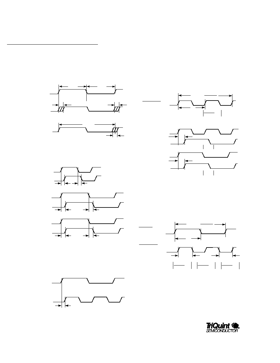
Switching Waveforms
Figure 3. General Timing
t PD1,2
t JR
tCPW
(INDIVIDUALLY)
REFCLK
FBIN
Q0 ≠ Q10
tCPW
t PERIOD
t JP
Figure 6. t
SKEW3
Figure 4. t
SKEW1
Group A
Group A
Group B
Group B
Group C
Group C
t SKEW1
t SKEW1
t SKEW1
t SKEW1
t SKEW1
t SKEW1
t SKEW2
Group B
Group A
t SKEW4 = Period
2
≠ t
=
Period
4
≠ t
=
Period
4
≠ t
t 3
t 4
Groups B, C
Group A
Period =
1
f
REFCLK
t 2
f = f
f = 2x f
REF
REF
2
3
4
(For Group B Feedback)
(For Group A or B Feedback)
Note:"n" is the phase-shift increment: 2t, t, ≠t, ≠2t.
Figure 7. t
SKEW4
Figure 5. t
SKEW2
GA1085
SYSTEM TIMING
SYSTEM TIMING
PRODUCTS
7
For additional information and latest specifications, see our website: www.triquint.com
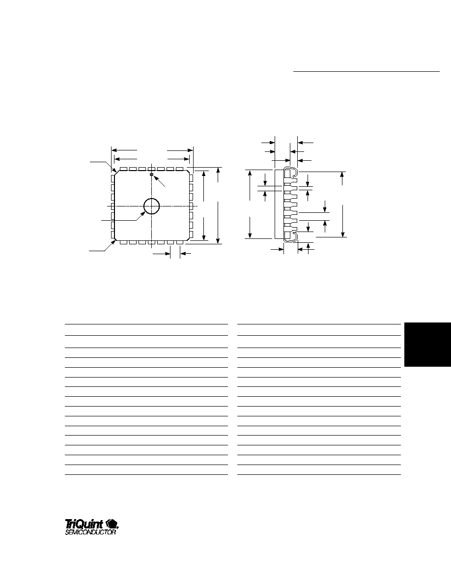
28-Pin MQuad Pin Description
Pin #
Pin Name
Description
I/O
1
GND
Ground
--
2
Q9
Output Clock 9 (C1)
O
3
Q10
Output Clock 10 (C2)
O
4
VDD
+5 V
--
5
GND
Ground
--
6
F0
Frequency Select 0
I
7
F1
Frequency Select 1
I
8
S0
Shift Select 0
I
9
REFCLK
Reference Clock
I
10
S1
Shift Select 1
I
11
FBIN
Feedback In
I
12
TEST
Test
I
13
VDD
+5 V
--
14
Q0
Output Clock 0 (B1)
O
PIN 1
.050 TYP.
NON-ACCUM.
.445 ±.005
.490 ±.005
.445
±.005
.490
±.005
.045
X 45∞∞
.132 ±.005
.050 TYP.
.410
±.015
.018
.104
±.005
.172 ±.005
8
15
22
.445
±.005
.040 MIN
.015
X 45∞∞
0.125
VENT PLUG
.028
.060
(All dimensions are in inches)
28-Pin MQuad J-Leaded Package Mechanical Specification
Pin #
Pin Name
Description
I/O
15
GND
Ground
--
16
Q1
Output Clock 1 (B2)
O
17
Q2
Output Clock 2 (B3)
O
18
VDD
+5 V
--
19
GND
Ground
--
20
Q3
Output Clock 3 (B4)
O
21
Q4
Output Clock 4 (A1)
O
22
VDD
+5 V
--
23
Q5
Output Clock 5 (A2)
O
24
Q6
Output Clock 6 (A3)
O
25
GND
Ground
--
26
VDD
+5 V
--
27
Q7
Output Clock 7 (A4)
O
28
Q8
Output Clock 8 (A5)
O
GA1085
For additional information and latest specifications, see our website: www.triquint.com
8
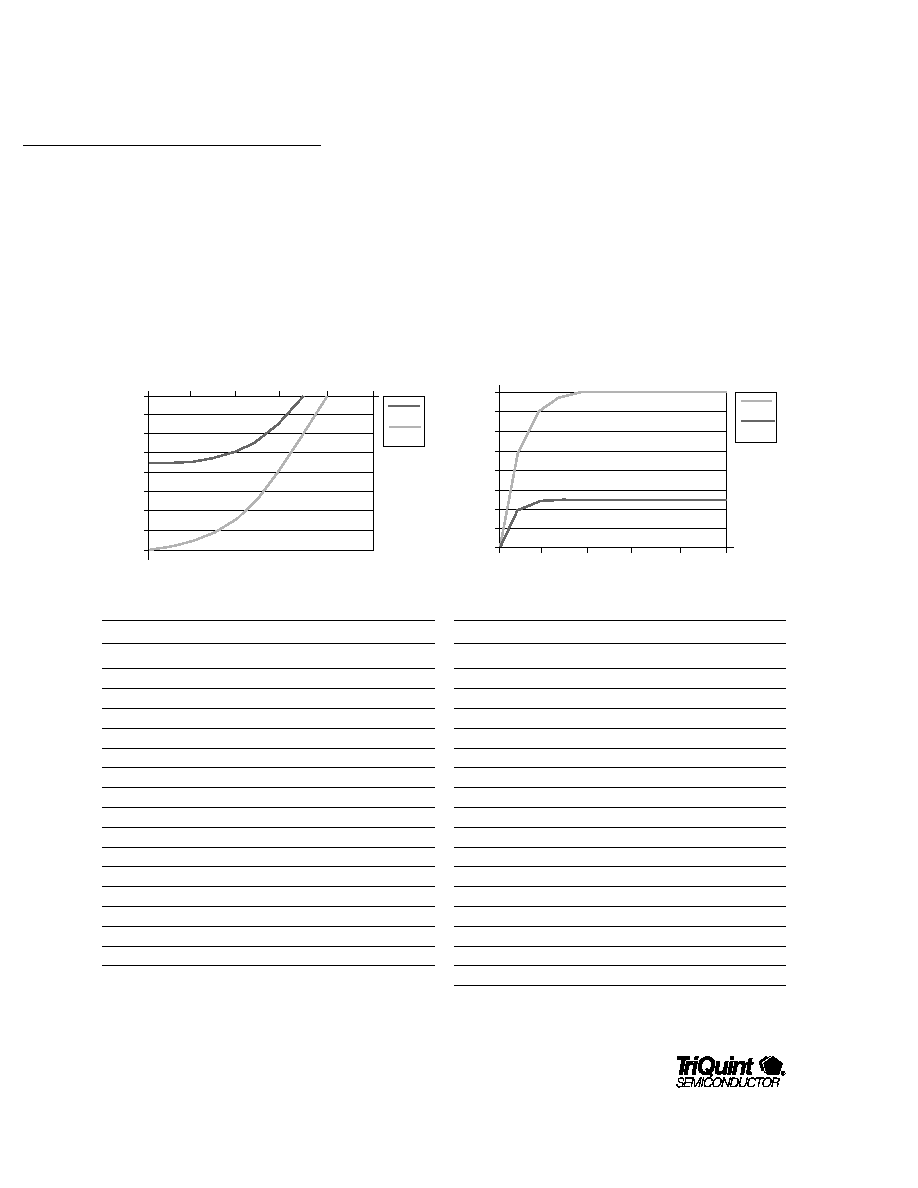
Output Characteristics
Figure 9. I
OH
vs.V
OH
Table 4. I
OH
vs.V
OH
V
OH
I
OH
min (mA)
I
OH
max (mA)
0.0
≠70
≠160
0.5
≠70
≠157
1.0
≠68
≠152
1.5
≠65
≠142
2.0
≠59
≠130
2.5
≠48
≠106
3.0
≠29
≠79
3.5
0
≠42
4.0
0
0
4.5
0
0
5.0
0
0
6.0
0
0
7.0
0
0
8.0
0
0
9.0
0
1
10.0
0
5
Table 5. I
OL
vs.V
OL
Figure 10. I
OL
vs.V
OL
0.0 1.0 2.0 3.0 4.0 5.0
Volts
0
-20
-40
-60
-80
-100
-120
-140
-160
I (mA)
OH
V max
OH
V min
OH
HIGH
0.0 1.0 2.0 3.0 4.0 5.0
Volts
160
140
120
100
80
60
40
20
0
I (mA)
OL
V max
OL
V min
OL
LOW
The IV characteristics, transition times, package
characteristics, device and bond-wire characteristics
for the GA1085 are described in Tables 4 through 9 and
Figures 9 through 11.
These output characteristics are provided for
modelling purposes only. TriQuint does not guarantee
the information in these tables and figures.
Notes:
1. These are worst-case corners for process, voltage,
and temperature.
2. Includes diode to ground current.
V
OL
I
OL
min (mA)
I
OL
max (mA)
≠2.5
≠145
≠435
≠2.0
≠135
≠410
≠1.5
≠115
≠350
≠1.0
≠90
≠265
≠0.5
≠40
≠120
0.0
0
0
0.5
37
97
1.0
49
140
1.5
53
155
2.0
54
157
2.5
54
159
3.0
54
160
3.5
54
160
4.0
54
160
4.5
54
160
5.0
54
160
10.0
54
160
GA1085
SYSTEM TIMING
SYSTEM TIMING
PRODUCTS
9
For additional information and latest specifications, see our website: www.triquint.com
Diode to GND
Diode Stack to VDD
V
I (mA)
V
I (mA)
0.0
0
5.0
0
≠0.4
0
6.0
0
≠0.5
0
7.0
0
≠0.6
≠5
8.0
0
≠0.7
≠15
9.0
0
≠0.8
≠35
10.0
1
≠0.9
≠55
11.0
5
≠1.0
≠75
12.0
9
≠2.0
≠300
≠2.5
≠350
≠3.0
≠360
Note: TriQuint does not guarantee diode operation for purposes other
than ESD protection.
Table 6. Characteristics Above V
DD
and Below Ground
L2
C2
1.85 nH
0.40 pF
Table 9. Rise and Fall Times
Figure 11. Output Model
C2
DIE
C1
L2
L1
OUTPUT
Time (ns) T
R
min (V) T
R
max (V) T
F
min (V) T
F
max (V)
0.0
0.15
0.32
3.20
3.04
0.1
0.15
0.32
3.20
3.04
0.2
0.16
0.32
3.06
2.95
0.3
0.18
0.32
2.86
2.90
0.4
0.23
0.32
2.62
2.68
0.5
0.26
0.32
2.38
2.50
0.6
0.34
0.32
2.17
2.36
0.7
0.46
0.34
2.00
2.22
0.8
0.67
0.39
1.85
2.09
0.9
0.89
0.49
1.69
1.95
1.0
1.12
0.63
1.52
1.86
1.1
1.32
0.86
1.38
1.68
1.2
1.50
1.09
1.26
1.59
1.3
1.73
1.27
1.12
1.49
1.4
1.93
1.45
0.96
1.36
1.5
2.15
1.64
0.83
1.23
1.6
2.75
2.23
0.52
0.95
1.7
2.58
2.00
0.61
1.00
1.8
2.75
2.23
0.52
0.95
1.9
2.90
2.41
0.45
0.91
2.0
3.02
2.50
0.39
0.86
2.1
3.12
2.64
0.33
0.77
2.2
3.17
2.77
0.29
0.73
2.3
3.19
2.86
0.24
0.68
2.4
3.20
2.95
0.21
0.64
2.5
3.20
2.99
0.19
0.59
2.6
3.20
3.02
0.17
0.55
2.7
3.20
3.02
0.16
0.53
2.8
3.20
3.04
0.16
0.50
2.9
3.20
3.04
0.15
0.45
3.0
3.20
3.04
0.15
0.41
3.1
3.20
3.04
0.15
0.40
3.2
3.20
3.04
0.15
0.37
3.3
3.20
3.04
0.15
0.36
3.4
3.20
3.04
0.15
0.32
3.5
3.20
3.04
0.15
0.32
Table 7. Device and Bond-Wire Characteristics
(Estimates)
L1
C1
2 nH
10 pF
Table 8. 28-Pin MQuad Package Characteristics
(Into 0 pF, 50 Ohms to 1.5 V)
GA1085
For additional information and latest specifications, see our website: www.triquint.com
10
Ordering Information
To order, please specify as shown below:
GA1085-MC nnnn
11-Output Configurable Clock Buffer
Propagation delay skew:
1000
= ≠350 ps
±
1000 ps
Temperature range: Commercial (0
∞
C to 70
∞
C)
Package: MQuad
For latest specifications, additional product information,
worldwide sales and distribution locations, and information about TriQuint:
Web: www.triquint.com
Tel: (503) 615-9000
Email: sales@tqs.com
Fax: (503) 615-8900
For technical questions and additional information on specific applications:
Email: applications@tqs.com
The information provided herein is believed to be reliable; TriQuint assumes no liability for inaccuracies or
omissions. TriQuint assumes no responsibility for the use of this information, and all such information
shall be entirely at the user's own risk. Prices and specifications are subject to change without notice.
No patent rights or licenses to any of the circuits described herein are implied or granted to any third party.
TriQuint does not authorize or warrant any TriQuint product for use in life-support devices and/or systems.
Copyright © 1997 TriQuint Semiconductor, Inc. All rights reserved.
Revision 1.1.A
November 1997