 | –≠–ª–µ–∫—Ç—Ä–æ–Ω–Ω—ã–π –∫–æ–º–ø–æ–Ω–µ–Ω—Ç: GA1086 | –°–∫–∞—á–∞—Ç—å:  PDF PDF  ZIP ZIP |
T
R
I Q
U
I
N
T
S E M I C O N D U C T O R , I N C .
SYSTEM TIMING
PRODUCTS
1
For additional information and latest specifications, see our website: www.triquint.com
GA1086
11-Output
Clock Buffer
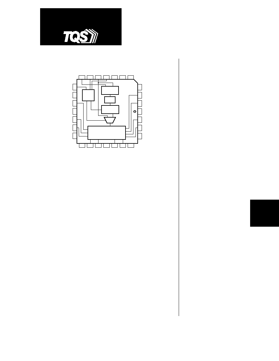
Figure 1. Block Diagram
TriQuint's GA1086 operates from 30 MHz to 67 MHz. This TTL-level clock
buffer chip supports the tight timing requirements of high-performance
microprocessors, with near zero input-to-output delay and very low pin-to-
pin skew. The device offers 10 usable outputs synchronized in phase and
frequency to a periodic clock input signal. One of the ten outputs is a one-
half clock output (CLK
˜
2). With split termination, the GA1086 can be
used to drive up to nineteen 15 pF loads, as shown in Figure 10.
The tight control over phase and frequency of the output clocks is achieved
with a 400 MHz internal Phase-Locked Loop (PLL). By feeding back one of
the output clocks to FBIN, the on-chip PLL continuously maintains
synchronization between the input clock (CLK) and all ten outputs. Any
drift or gradual variation in the system clock is matched and tracked at the
ten outputs. The GA1086 output buffers are symmetric, each sourcing and
sinking up to 30 mA of drive current. For diagnostic purposes, the device
has a test mode which is used to test the device and associated logic by
single-stepping through the control logic.
The GA1086 is fabricated using TriQuint's One-UpTM gallium arsenide
technology to achieve precise timing control and to guarantee 100% TTL
compatibility. The output frequency makes this device ideal for clock
generation and distribution in a wide range of high-performance
microprocessor-based systems. Many other CISC- and RISC-based
systems will also benefit from its tight control of skew and delay.
Precision
Output
Buffers
MUX
Divide
Logic
VCO
Phase
Detector
Control
Logic
VDD
Q9
Q8
GND
Q7
Q6
VDD
S2
VDD
Q/2
GND
FBOUT
Q1
VDD
FBIN S1 CLK S0 NC NC GND
GND Q2 Q3 VDD Q4 Q5 GND
1
2
14
13
12
4
3
22
21
20
19
18
17
16
15
27
28
25
24
23
26
11
10
9
8
7
6
5
Features
∑
Operates from 30 MHz to 67 MHz
∑
Pin-to-pin output skew of
250 ps (max)
∑
Period-to-period jitter:
75 ps (typ)
∑
Near-zero propagation delay:
≠350 ps
±
500 ps or
≠350 ps
±
1000 ps
∑
10 symmetric, TTL-compatible
outputs with 30 mA drive and
rise and fall times of 1.4 ns(max)
∑
28-pin J-lead surface-mount
package
∑
Special test mode
∑
Meets or exceeds Pentium
TM
processor timing requirements
∑
Typical applications include
low-skew clock distribution for:
∑
RISC- or CISC-based systems
∑
Multi-processor systems
∑
High-speed backplanes

GA1086
For additional information and latest specifications, see our website: www.triquint.com
2
control bit settings, divide mode and VCO range.
FBOUT is fed back to FBIN and has the same frequency
as the Qn outputs.
The GA1086 has a test mode that allows for single
stepping of the clock input for testing purposes. With
S2 HIGH, S1 LOW and S0 HIGH, the signal at the CLK
input goes directly to the outputs, bypassing the PLL
circuitry.
The maximum rise and fall time at the output pins is 1.4
ns. All outputs of the GA1086 are TTL-compatible with 30
mA symmetric drive and a minimum V
OH
of 2.4 V.
The GA1086-MC500 and GA1086-MC1000 are identical
except for the propagation delay specification (see AC
Characteristics table).
Breaking the Feedback Loop
There is no requirement that the external feedback
connection be a direct hardwire from an output pin to
the FBIN pin. As long as the signal at FBIN is derived
directly from the FBOUT pin and maintains its
frequency, additional delays can be accommodated.
The internal phase-locked loop will adjust the output
clocks on the GA1086 to ensure zero phase delay
between the FBIN and CLK signals.
Note: the signal at FBIN must be continuous, i.e. not a gated or
conditional signal.
Functional Description
The GA1086 generates 10 outputs (Q1 ≠ Q9 and
FBOUT) which have the same frequency and zero phase
delay relative to the reference clock input. In addition,
there is one output (Q/2) that has
1
/
2
the frequency of
the reference clock. The GA1086 maintains frequency
and zero phase delay using a Phase Detector to
compare the output clock with the reference clock
input. Phase deviations between the output clock and
reference clock are continuously corrected by the PLL.
Figure 1 shows a block diagram of the PLL, which
consists of a Phase Detector, Voltage Controlled
Oscillator (VCO), Divide Logic, Mux and Control Logic.
The Phase Detector monitors the phase difference
between FBIN which is connected to FBOUT, and the
reference clock (CLK). The Phase Detector adjusts the
VCO such that FBIN aligns with CLK. The VCO has an
operating range of 360 MHz to 402 MHz. The output
clocks (Qn, FBOUT, and Q/2) are generated by dividing
the VCO output.
The desired operating frequency determines the proper
divide mode. There are 4 divide modes;
˜
12,
˜
10,
˜
8
and
˜
6. In each mode, the GA1086 operates across the
frequency range listed in the Divide Mode Selection
Table. The operating frequency is equivalent to the VCO
frequency divided by the mode number.
Table 1 shows the input clock frequency (CLK), output
clock frequency (Qn),
1
/
2
output clock frequency (Q/2),
Table 1. Divide Mode Selection Table
Control
Divide
CLK
Qn
Q/2
S2
S1
S0
Mode
30 ≠ 33 MHz
30 ≠ 33 MHz
15 ≠ 16.5 MHz
1
1
1
˜
12
36 ≠ 40 MHz
36 ≠ 40 MHz
18 ≠ 20 MHz
1
1
0
˜
10
45 ≠ 50 MHz
45 ≠ 50 MHz
22.5 ≠ 25 MHz
1
0
0
˜
8
60 ≠ 67 MHz
60 ≠ 67 MHz
30 ≠ 33.5 MHz
0
1
1
˜
6
TSTCLK
TSTCLK
TSTCLK/2
1
0
1
--
GA1086
SYSTEM TIMING
PRODUCTS
3
For additional information and latest specifications, see our website: www.triquint.com
Power-Up/Reset Synchronization
The GA1086 utilizes on-chip phase-locked loop (PLL)
technology to maintain synchronization between inputs
and outputs. Whenever the device is powered up, or
the system clock (CLK) is reset, the phase-locked loop
requires a synchronization time (t
SYNC
) before lock is
achieved. The maximum time required for
synchronization is 500 ms.
Typical Applications
The GA1086 is designed to satisfy a wide range of
system clocking requirements. Following are two of the
most common clocking bottlenecks which can be
solved using the GA1086.
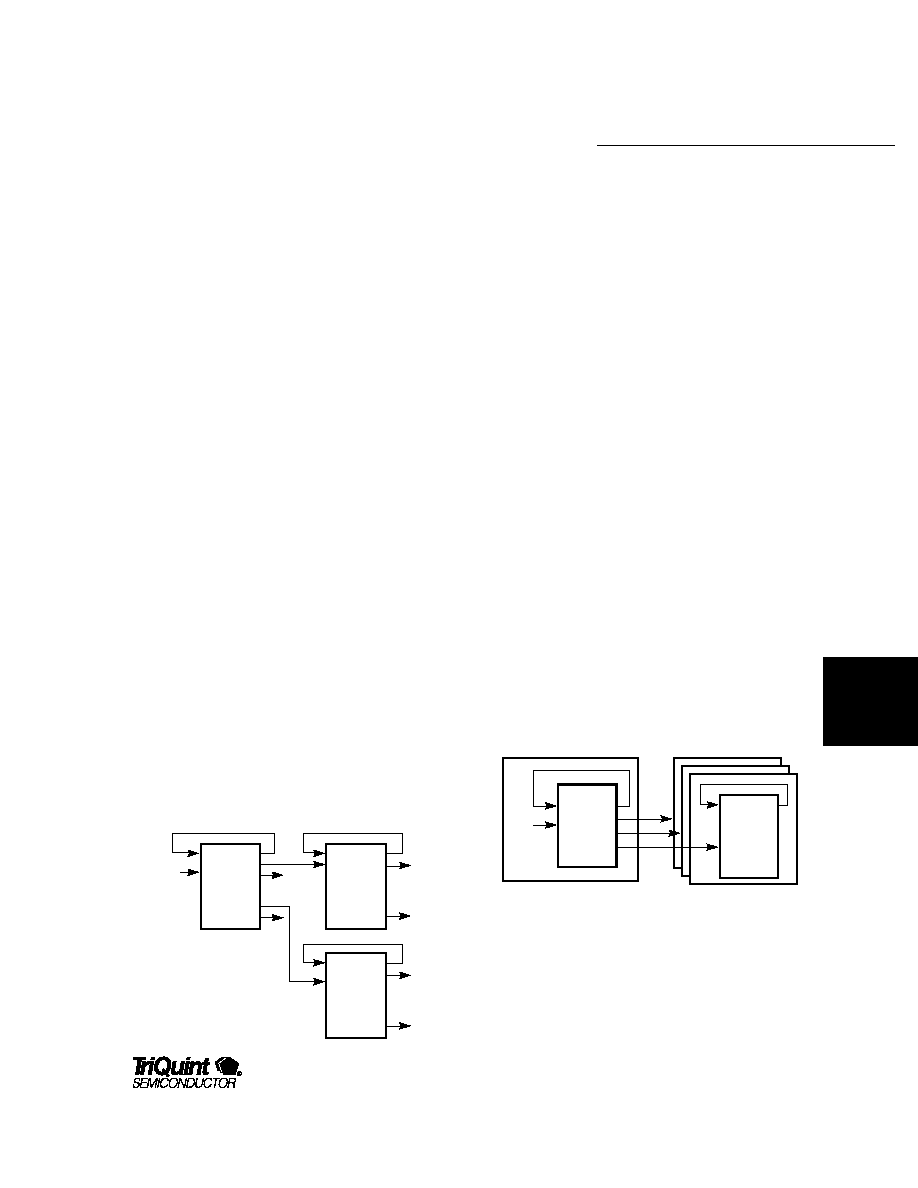
1) Low-Skew Clock Distribution / Clock Trees
The most basic bottleneck to clocking high-performance
systems is generating multiple copies of a system clock,
while maintaining low skew throughout the system.
∑ The GA1086 guarantees low skew among all clocks
in the system by controlling both the input-to-
output delay and the skew among all outputs. In
Figure 2, the worst-case skew from Output 1 to
Output n, with reference to the system clock, is
Figure 2. Low-Skew Clock Distribution
Figure 3. Board-to-Board Synchronization
GA1086
(1)
GA1086
(2)
GA1086
(n)
SYSTEM
CLOCK
∑
∑
∑
∑
∑
∑
∑
∑
∑
Q1
Q9
Q/2
OUTPUT 1
OUTPUT n
Q1
SYS
CLK
GA1000
GA1086
HOST
TARGETS
t
≠t
≠2t
GA1110E
obtained by summing the various skews. The skew
between the outputs of the GA1086 (1) which drive
the GA1086 (2) and the GA1086 (n) is summed
with the propagation delay of the GA1086 (2 or n),
the skew between the outputs of the GA1086 (2),
and the skew between the outputs of the GA1086
(n). This results in a total skew of 1.75 ns (250 ps +
1000 ps + 250 ps + 250 ps).
2) Board-to-Board Synchronization
Many computing systems today consist of multiple
boards designed to run synchronously. The skew
associated with routing clocks across a backplane
presents a major hurdle to maximizing system
performance.
∑ The edge placement feature of TriQuint's
configurable custom clock generator (GA1110E)
operating at 33 MHz, coupled with the tightly
controlled input/output delay of the GA1086,
ensures all boards in the system are running
synchronously.

GA1086
For additional information and latest specifications, see our website: www.triquint.com
4
Multi-Processor Systems
The GA1086 can be effectively used to distribute clocks
in RISC- or CISC-processor-based systems. Its 10
outputs support both single- and multi-processor
systems. Following are three representative
configurations which show how the 10 outputs can be
used to synchronize the operation of CPU cache and
memory banks operating at different speeds.
CPU 1
CACHE
MEMORY
CONTROL
LOGIC
(66 MHZ)
SLOW
MEMORY
CONTROL
LOGIC
(33 MHZ)
CPU 2
CACHE
SYSTEM
CLOCK
GA1086
R
R
R
R
R
FBOUT
Q1
Q2
Q3
Q4
Q5
Q6
Q7
Q8
Q9
Q/2
R
R
R
R
R
R
FBIN
CLK
S2
S1
S0
LOW
HIGH
HIGH
Figure 4. Clocking a Dual-CPU System
Figure 4 depicts a 2-CPU system in which the
processors and associated peripherals are operating at
66 MHz. Each of the nine outputs operating at 66 MHz
are fully utilized to drive the appropriate CPU, cache,
and memory control logic. The 33 MHz output is used
to synchronize the operation of the slower memory
bank to the rest of the system.
GA1086
SYSTEM TIMING
PRODUCTS
5
For additional information and latest specifications, see our website: www.triquint.com
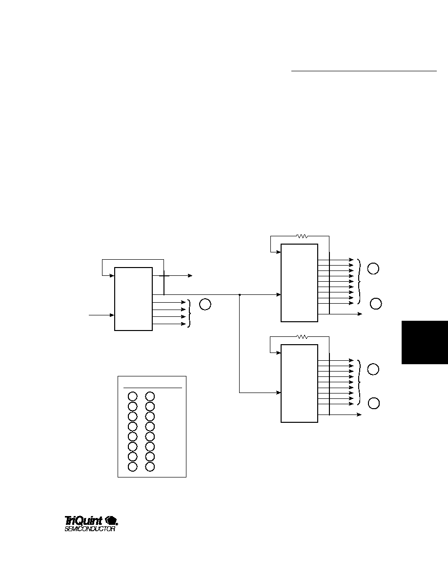
Multi-Processor Systems (cont.)
Figure 5 shows a 4-processor system with various
33 MHz memory banks synchronized to the 66 MHz
CPUs. The GA1110E, a custom device whose six
outputs can be individually configured, (see
GA1110E data sheet), is used as the clock source for
the GA1086 devices. This configuration gives the user
18 copies of the 66 MHz clock and 7 copies of the 33
MHz clock. By using the configurability of the
GA1110E, the user can also specify and control the
placement of the edges of the outputs of the GA1110E.
Figure 5. Generating Multiple Outputs
FBIN
GA1000
CLK
FBOUT
Q1
Q2
Q3
Q4
Q5
33 MHz
FBIN
GA1086
MC500
CLK
FBOUT
Q1
Q9
Q/2
R
6 pF
1
9 @ 66 MHz
2
FBIN
GA1086
MC500
CLK
FBOUT
Q1
Q9
Q/2
R
6 pF
4
9 @ 66 MHz
5
33 MHz
33 MHz
66 MHz
Note: The GA1000 is a custom device whose outputs
can be customized to the user's requirement.
The figure above is one possible configuration.
33 MHz
3
4 @ 33 MHz
≠ t
≠ 2t
≠ 3t
*
Assumes maximum skew between Q9 and Q/2 is 1.2 ns. See AC specifications.
Max Pin-to-Pin Skew from:
2
1
3
1
4
1
3
2
to = 1.2 ns*
to = 1.75 ns
to = 1.5 ns
to = 2.7 ns*
to = 3.2 ns*
to = 1.75 ns
to = 2.7 ns*
to = 1.2 ns*
5
2
4
3
5
3
5
4
33MHz
GA1110E

GA1086
For additional information and latest specifications, see our website: www.triquint.com
6
Single-Processor Systems
Figure 6 is an example of a single-CPU system. The
nine 66MHz outputs of the GA1086 are used to drive
the CPU and its related cache, the state machine,
memory banks, and other general-purpose logic.
CPU
CACHE
LOGIC
BLOCK 2
LOGIC
BLOCK 1
MEMORY
CONTROL
STATE
MACHINE
GA1086
R
R
R
R
R
FBOUT
Q1
Q2
Q3
Q4
Q5
Q6
Q7
Q8
Q9
Q/2
R
R
R
R
R
R
FBIN
CLK
S2
S1
S0
SYSTEM
CLOCK
LOW
HIGH
HIGH
Figure 6. Clocking a Single-CPU System
The table in Figure 5 also specifies the maximum pin-
to-pin skew of various sets of outputs from the three
clocking devices.
Please note that the GA1086s are series-terminated and
that the feedback trace lengths for the two devices
should be equal.
GA1086
SYSTEM TIMING
PRODUCTS
7
For additional information and latest specifications, see our website: www.triquint.com
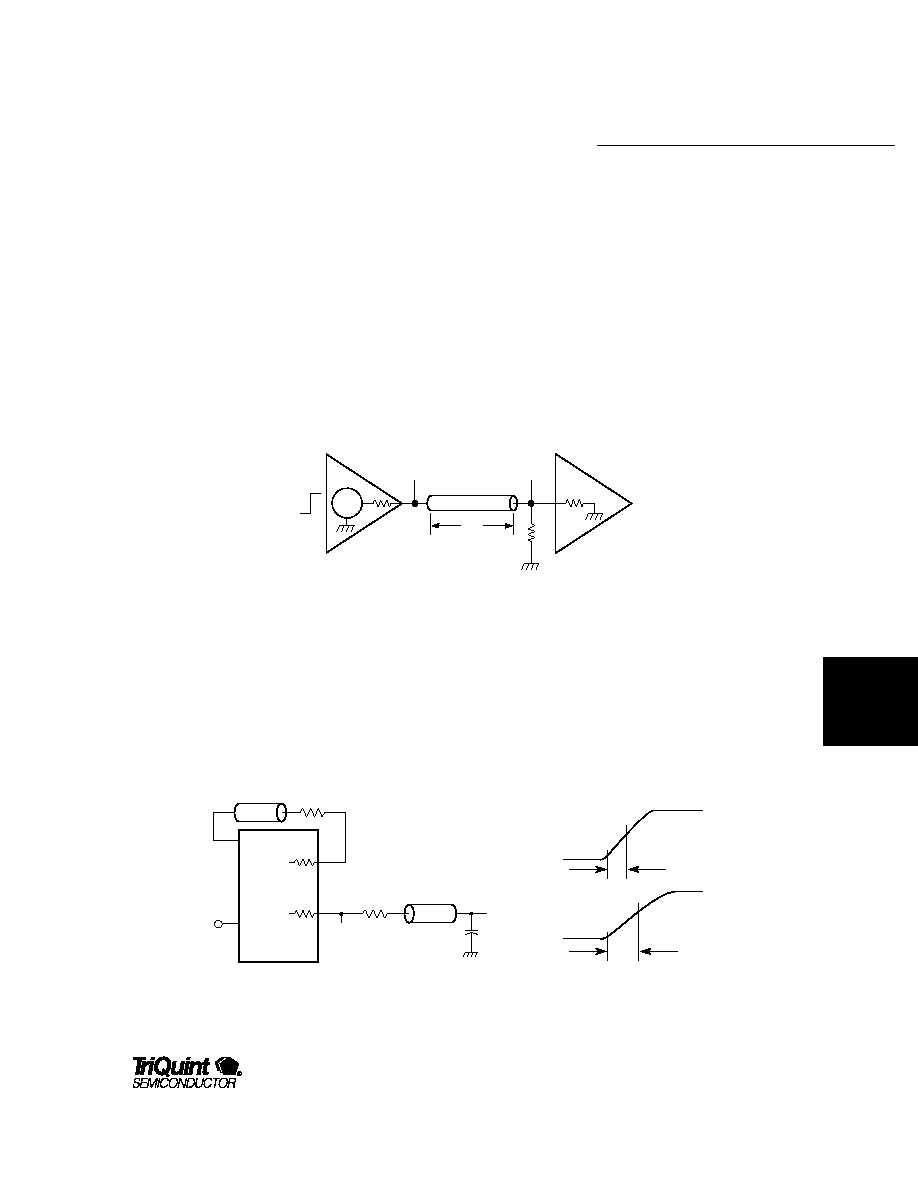
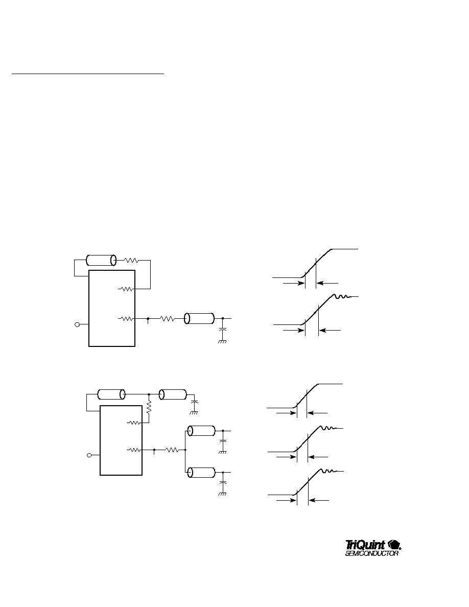
Parallel Termination of Outputs
The GA1086 can be terminated either in parallel or in
series. If power dissipation is not of primary concern,
then parallel termination can be the most effective
mode of termination for the GA1086. An example of
this termination is shown in Figure 7, along with the
waveforms at an output pin and at the load. Note that
the Thevenin equivalent using two resistors and +5 V
supply can replace the 65 ohms to 1.5 V.
Unused outputs must be terminated.
Qt
0
52
65
Qt
1
30 pF
1.4 ns (max)
Qt
0
1.8 ns (typ)
Qt
1
65
52
CLK
GA1086
13
13
Q
FBIN
FBOUT
Figure 8. Balanced Termination
Series Termination of Outputs
The alternative to parallel termination is series
termination. For applications where overshoots and
undershoots of the clock signal are a concern, it is best
Figure 7. Parallel Termination
to use balanced termination as shown in Figure 8. This
could, however, slow the rise time of the pulses
arriving at the destination.
Z
O
t
AB
A
R
OUT
R
T
V
OUT
B
R
IN
GA1086
For additional information and latest specifications, see our website: www.triquint.com
8
Qt
0
12
1.4 ns (max)
Qt
0
1.5 ns (typ)
1.5 ns (typ)
Qt
1
65
Qt
2
15 pF
65
Qt
1
15 pF
Qt
2
65
15 pF
12
65
CLK
GA1086
13
13
Q
FBIN
FBOUT
Figure 10. Split Unbalanced Termination
If rise times are critical and if overshoots and
undershoots can be tolerated, then unbalanced
termination may be used. Reflections due to
unbalanced termination can cause ringing at the load.
The transmission line lengths, therefore, must be long
enough to cause the ringing to occur only after the
waveform has completely switched to either the LOW
or the HIGH state, (the round trip). The propagation
time of the output signals should be greater than the
switching time for LOW to HIGH or HIGH to LOW.
Qt
0
37
65
Qt
1
30 pF
1.4 ns (max)
Qt
0
1.5 ns (typ)
Qt
1
65
37
CLK
GA1086
13
13
Q
FBIN
FBOUT
Figure 9. Unbalanced Termination
To double the number of loads (devices) driven by the
GA1086, split termination may be used. Examples of
three types of series termination and the resulting
waveforms, measured between 0.8 V and 2.0 V, are
shown in Figures 9 and 10 for one of the outputs.
Unused outputs must be terminated.
Note: Rise time at Q
t1
is measured between 0.8 V and 2.0 V.
GA1086
SYSTEM TIMING
PRODUCTS
9
For additional information and latest specifications, see our website: www.triquint.com
Caution: Damage to the device may occur if an output is shorted to ground or V
DD
.
Notes: 1. These values apply to both the GA1086-MC500 and GA1086-MC1000.
2. Typical limits are at V
DD
= 5.0 V and T
A
= 25
∞
C.
3. These are absolute values with respect to device ground and all overshoots due to system or tester noise are included.
4. I
DD
is measured with outputs LOW and unloaded.
5. These parameters are not 100% tested, but are periodically sampled.
Limits
2
Symbol
Description
Test Conditions
Min
Typ
Max
Unit
V
OH
Output HIGH voltage
V
DD
= Min
I
OH
= ≠30 mA
2.4
3.6
V
V
IN
= V
IH
or V
IL
V
OL
Output LOW voltage
V
DD
= Min
I
OL
= 30 mA
0.2
0.5
V
V
IN
= V
IH
or V
IL
V
IH
3
Input HIGH level
Guaranteed input logical HIGH
2.0
V
voltage for all inputs
V
IL
3
Input LOW level
Guaranteed input logical LOW
0.8
V
voltage for all inputs
I
IL
Input LOW current
V
DD
= Max
V
IN
= 0.40 V
≠166
≠400
µ
A
I
IH
Input HIGH current
V
DD
= Max
V
IN
= 2.7 V
0
25
µ
A
I
I
Input HIGH current
V
DD
= Max
V
IN
= 5.5 V
2
1000
µ
A
I
DD
4
Power supply current
V
DD
= Max
115
160 mA
V
I
Input clamp voltage
V
DD
= Min
I
IN
= ≠18 mA
≠0.62
≠1.2
V
Symbol
Description
Test Conditions
Min
Typ
Max
Unit
C
IN
Input capacitance
V
IN
= 2.0 V at f = 1 MHz
6
pF
DC Characteristics
(Supply voltage: +5 V + 5% Ambient temp: 0
∞
C to +70
∞
C)
1
Capacitance
1,5
Storage temperature
≠65
∞
C to +150
∞
C
Ambient temperature with power applied
≠55
∞
C to +100
∞
C
Supply voltage to ground potential
≠0.5 V to +7.0 V
DC input voltage
≠0.5 V to +(V
DD
+ 0.5)
DC input current
≠30 mA to +5 mA
Absolute Maximum Ratings
GA1086
For additional information and latest specifications, see our website: www.triquint.com
10
AC Specifications
Notes:
Q0
Q1
Q2
∑
∑
∑
∑
Q10
FBIN
CLK
∑
∑
∑
∑
R1
R2
+5 V
R1
R2
+5 V
R1
R2
+5 V
R1
R2
+5 V
R1
R2
+5 V
Y
X
50
Z
Z
R1 = 160
R2 = 71
Y + Z = X
Input Clocks
Min
Typ
Max
Unit
F
IN
CLK frequency
30
--
67
MHz
t
CP
CLK period
14.9
--
33
ns
t
CPW
CLK pulse width
3.0
--
--
ns
t
IR
Input rise time
(0.8 V ≠ 2.0 V)
--
--
2.0
ns
Output Clocks
Min
Typ
Max
Unit
t
OR
Output rise time
(0.8 V ≠ 2.0 V)
0.15
--
1.4
ns
t
OF
Output fall time
(0.8 V ≠ 2.0 V)
0.15
--
1.4
ns
t
PD1
1
CLK Œ to FBIN Œ
(MC500)
≠850
≠350
+150
ps
t
PD2
1,2
CLK Œ to FBIN Œ
(MC1000)
≠1350
≠350
+650
ps
t
SKEW1
2,3
Q1≠Q9 and FBOUT
(0.8V)
≠125
--
+125
ps
t
SKEW1
2,3
Q1≠Q9 and FBOUT
(1.5V)
≠125
--
+125
ps
t
SKEW1
2,3
Q1≠Q9 and FBOUT
(2.0V)
≠125
--
+125
ps
t
SKEW2
2,3
Q/2 Output skew
--
0.6
1.2
ns
t
W
4
Output window
--
100
250
ps
t
CYC
5
Duty-cycle variation
--
1.0
--
ns
t
SYNC
6
Synchronization time
--
200
500
µ
s
t
JIT
7
Period-to-period jitter
--
75
--
ps
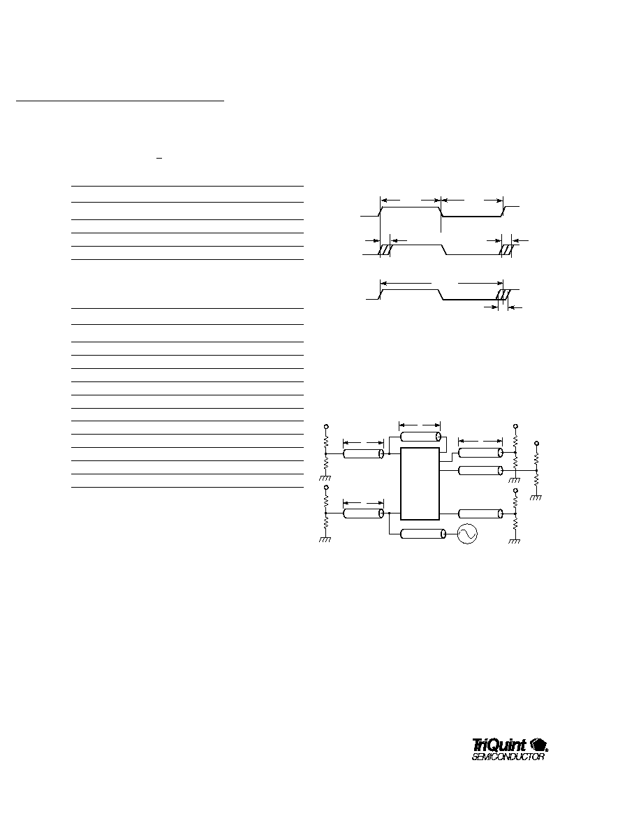
Figure 11. Switching Waveforms
Buffer Configuration (FBIN = FBOUT)
t PD1,2
t JR
tCPW
(INDIVIDUALLY)
REFCLK
FBIN
Q0 ≠ Q10
tCPW
t PERIOD
t JP
Figure 12. AC Test Circuit
(Supply voltage: +5 V + 5%, Ambient temp: 0
∞
C to +70
∞
C)
Notes: 1. The PLL maintains alignment of CLK and FBIN at all times. This specification applies to the rising edge only because the input duty
cycle can vary while the output duty cycle is typically 50/50. The delay t
PD
is measured at the 1.5 V level between CLK and FBIN.
2. t
PD
and t
SKEW
are tested with an input clock having a rise time of 0.5 ns (0.8 V to 2.0 V).
3. The output skew is measured from the middle of the output window, t
W
. The maximum skew is guaranteed across all voltages and
temperatures.
4. t
W
specifies the width of the window in which outputs Q1≠Q9 switch.
5. This specification represents the deviation from 50/50 on the outputs; it is sampled periodically but is not guaranteed.
6. t
SYNC
is the time required for the PLL to synchronize; this assumes the presence of a CLK signal and a connection from one of the
outputs to FBIN.
7. Jitter is specified as a peak-to-peak value.
GA1086
SYSTEM TIMING
PRODUCTS
11
For additional information and latest specifications, see our website: www.triquint.com
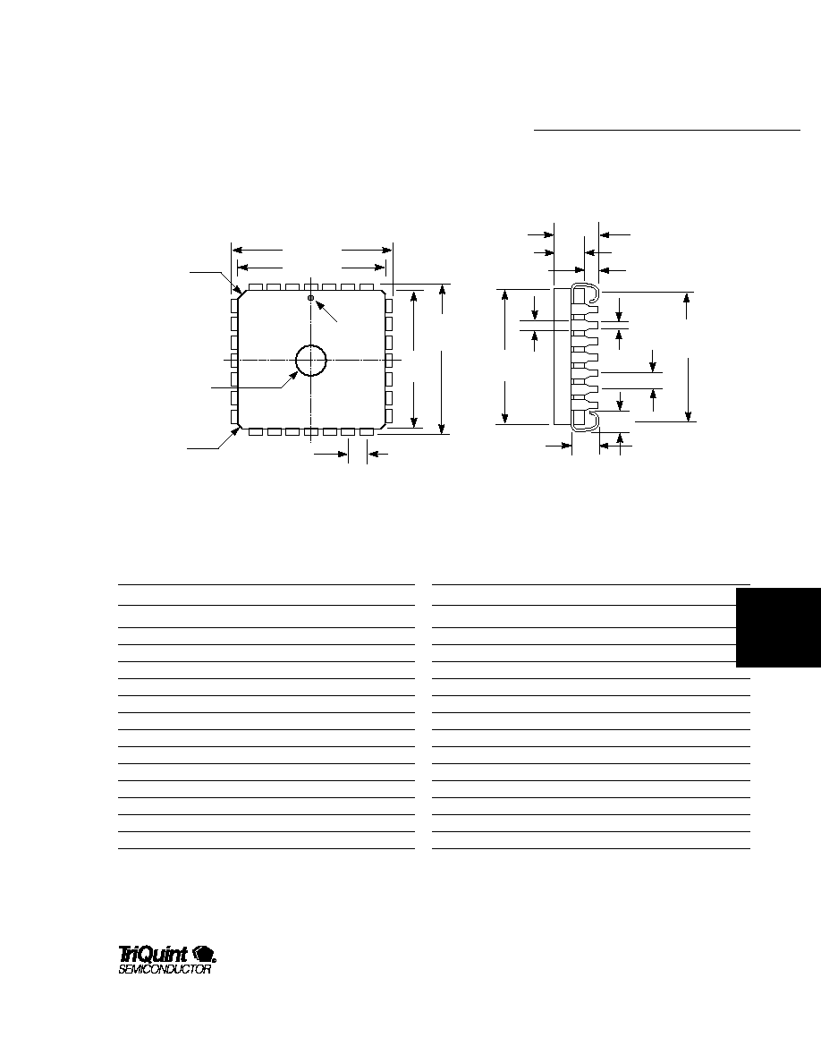
28-Pin MQuad J-Leaded Package Mechanical Specification
PIN 1
.050 TYP.
NON-ACCUM.
.445 ±.005
.490 ±.005
.445
±.005
.490
±.005
.045
X 45∞∞
.132 ±.005
.050 TYP.
.410
±.015
.018
.104
±.005
.172 ±.005
8
15
22
.445
±.005
.040 MIN
.015
X 45∞∞
0.125
VENT PLUG
.028
.060
Pin #
Pin Name
Description
I/O
1
GND
Ground
≠
2
Q8
Output Clock 8
O
3
Q9
Output Clock 9
O
4
VDD
+5 V
≠
5
GND
Ground
≠
6
N/C
No Connect
≠
7
N/C
No Connect
≠
8
S0
Select 0
I
9
CLK
Reference Clock
I
10
S1
Select 1
I
11
FBIN
Feedback In
I
12
S2
Select 2
I
13
VDD
+5 V
≠
14
Q/2
Half-Clock Out
O
28-Pin MQuad Pin Description
Pin #
Pin Name
Description
I/O
15
GND
Ground
≠
16
FBOUT
Feedback Clock
O
17
Q1
Output Clock 1
O
18
VDD
+5 V
≠
19
GND
Ground
≠
20
Q2
Output Clock 2
O
21
Q3
Output Clock 3
O
22
VDD
+5 V
≠
23
Q4
Output Clock 4
O
24
Q5
Output Clock 5
O
25
GND
Ground
≠
26
VDD
+5 V
≠
27
Q6
Output Clock 6
O
28
Q7
Output Clock 7
O
(All dimensions are in inches)
GA1086
For additional information and latest specifications, see our website: www.triquint.com
12
Additional Information
For latest specifications, additional product
information, worldwide sales and distribution locations,
and information about TriQuint:
Web: www.triquint.com
Tel: (503) 615-9000
Email: sales@tqs.com
Fax: (503) 615-8900
For technical questions and additional information on
specific applications:
Email: applications@tqs.com
The information provided herein is believed to be reliable; TriQuint assumes no liability for inaccuracies or
omissions. TriQuint assumes no responsibility for the use of this information, and all such information
shall be entirely at the user's own risk. Prices and specifications are subject to change without notice.
No patent rights or licenses to any of the circuits described herein are implied or granted to any third party.
TriQuint does not authorize or warrant any TriQuint product for use in life-support devices and/or systems.
Copyright © 1997 TriQuint Semiconductor, Inc. All rights reserved.
Revision 1.1.A
November 1997
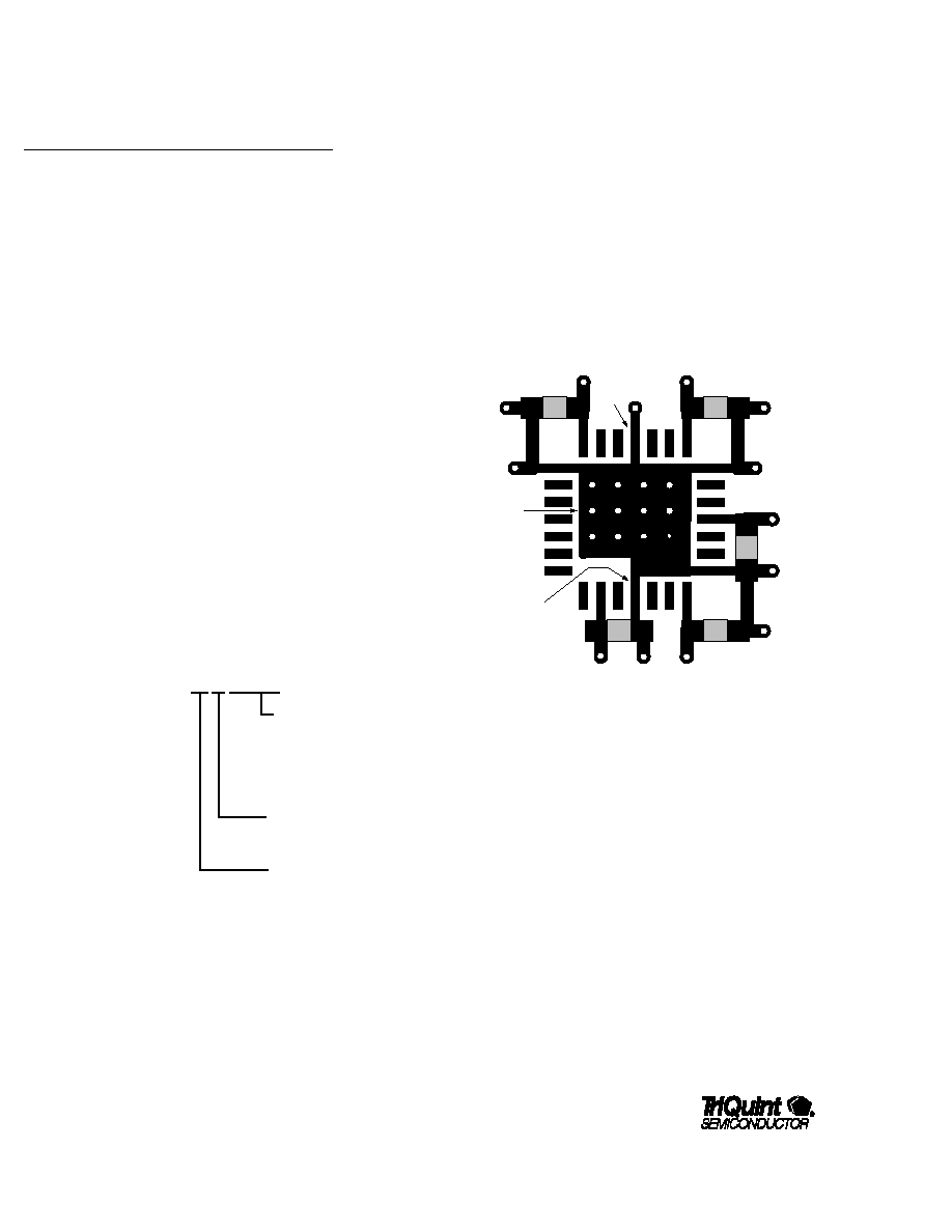
Layout Guidelines
Multiple ground and power pins on the GA1086 reduce
ground bounce. Good layout techniques, however, are
necessary to guarantee proper operation and to meet
the specifications across the full operating range.
TriQuint recommends bypassing each of the V
DD
supply
pins to the nearest ground pin, as close to the chip as
possible.
Figure 13 shows the recommended power layout for
the GA1086. The bypass capacitors should be located
on the same side of the board as the GA1086. The V
DD
traces connect to an inner-layer V
DD
plane. All of the
ground pins (GND) are connected to a small ground
plane on the surface beneath the chip. Multiple
C4
C5
C1
C2
C3
Pin 1
Pin 15
Ground
Plane
V
DD
V
DD
V
DD
V
DD
V
DD
Figure 13. Top Layer Layout of Power Pins
(Approx. 3.3x)
Package: MQuad
Ordering Information
To order, please specify as shown below:
GA1086-MC n...n
11-Output Clock Buffer
0
∞
C to 70
∞
C (Commercial)
through-holes connect this small surface plane to an
inner-layer ground plane. The capacitors (C1≠C5) are
0.1 mF. TriQuint's test board uses X7R temperature-
stable capacitors in 1206 SMD cases.
Propagation delay skew:
500
≠350 ps
±
500 ps
1000
≠350 ps
±
1000 ps
Temperature range: