 | –≠–ª–µ–∫—Ç—Ä–æ–Ω–Ω—ã–π –∫–æ–º–ø–æ–Ω–µ–Ω—Ç: IPHC | –°–∫–∞—á–∞—Ç—å:  PDF PDF  ZIP ZIP |

0.5-µm Intermediate-Profile, High-Current
MesFET (IPHC)
Process Data Sheet
Semiconductors for Communications, Space and Military
www.TriQuint.com
500 West Renner Road
Richardson, Texas 75080
Phone: 972-994-8200
Foundry: 972-994-4545
Email: info@triquint.com
Page 1 of 3; 9/24/02
Specifications are subject to change.
General Description
The 0.5-µm Intermediate-Profile, High-Current MesFET
(IPHC) process is a cost-effective 2MI (2-metal-interconnect)
depletion-mode ion-implant MesFET process for general-
purpose and high-power operation through 20 GHz. The
IPHC process allows for active switch, amplifier, and diode
integration. This process is typically used for amplifiers,
switches, doublers, mixers and VCO's in various applications.
Passives include 2 thick-metal interconnect layers, precision
TaN resistors, GaAs resistors, MIM capacitors, and through-
substrate vias. The via-under-cap process aids in size com-
paction and offers excellent grounds at higher frequencies.
Features
∑
0.5-µm amplifier transistors
∑
0.5-µm switch transistors
∑
0.5-µm diodes
∑
Device passivation
∑
High-Q passives
∑
MIM capacitors
∑
TaN resistors
∑
GaAs resistors
∑
2 metal layers
∑
Air bridges
∑
Substrate vias
∑
Operation up to V
d
= 8 V
Applications
∑
Up to 20 GHz
∑
Communications
∑
Space
∑
Military
∑
Power amplifiers
∑
Driver amplifiers
∑
AGC amplifiers
∑
Limiting amplifiers
∑
Transimpedance amplifiers
∑
Differential amplifiers
∑
Digital and analog phase shifters
∑
Digital and analog attenuators
∑
Mixers (up and down converters)
∑
Multipliers
∑
Switches
∑
Oscillators
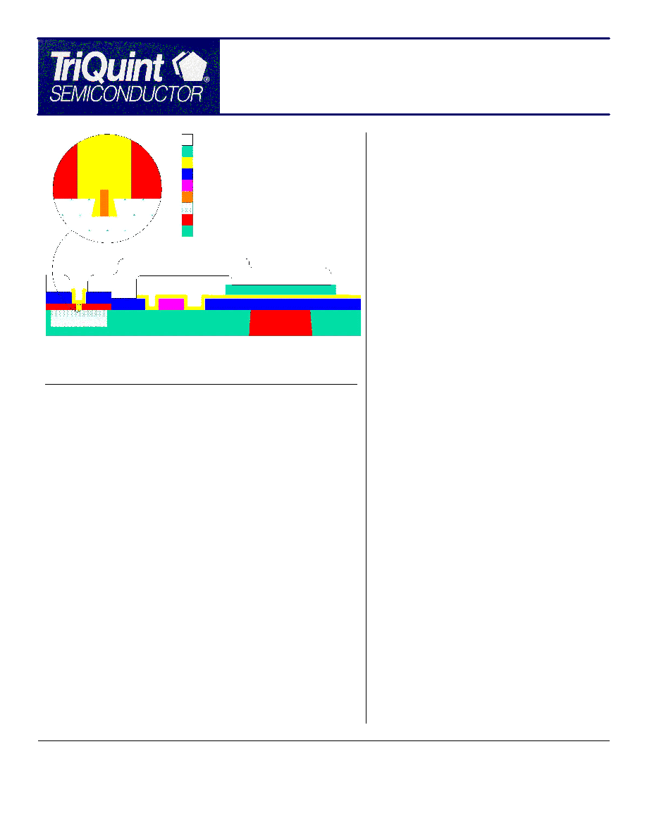
4.6 µm PLATING
CAP TOP PLATE
2000 ≈ NITRIDE
0.75 µm FIRST METAL
TaN RESISTOR
GATE
ACTIVE REGION
OHMIC METAL (EXCEPT VIA)
SEMI-INSULATING GaAs SUBSTRATE
VIA UNDER CAP
0.5-µm 2MI Process Cross Section

0.5-µm Intermediate-Profile, High-Current
MesFET (IPHC)
Process Data Sheet
Semiconductors for Communications, Space and Military
www.TriQuint.com
500 West Renner Road
Richardson, Texas 75080
Phone: 972-994-8200
Foundry: 972-994-4545
Email: info@triquint.com
Page 2 of 3; 9/24/02
Specifications are subject to change.
Application Examples
Gain Block Amplifier TGA8300-SCC:
The TriQuint TGA8300-SCC is a GaAs monolithic distributed amplifier designed for use as a
multi-octave general-purpose gain block.
6 to 18 GHz Power Amplifier TGA8014-SCC:
The TriQuint TGA8014-SCC is a two-stage GaAs monolithic medium-power amplifier which
provides 11-dB nominal gain with 16% typical power added efficiency and output power at 1-dB
gain compression of 0.5 Watt.
Gate Pitch (µm) Gate Fingers FET Sizes (µm)
26 26
4
300
38 38
10
600
FET Models Available (Noise)
Element
Parameter
Typical Value
Units
FETs
I
dss
320
mA/mm
G
m
165
mS/mm
V
bd
-14
V
V
p
-3
V
MIM capacitors
density
300
pF/mm
2
Capacitors over vias
yes
TaN resistors
sheet resistance
50
V
/sq
GaAs resistors
sheet resistance
325
V
/sq
Vias
yes
Substrate
thickness
100
µm
0.5-µm IPHC MesFET Process Details

0.5-µm Intermediate-Profile, High-Current
MesFET (IPHC)
Process Data Sheet
Semiconductors for Communications, Space and Military
www.TriQuint.com
500 West Renner Road
Richardson, Texas 75080
Phone: 972-994-8200
Foundry: 972-994-4545
Email: info@triquint.com
Page 3 of 3; 9/24/02
Specifications are subject to change.
Prototyping and Development
∑
Prototype Wafer Option (PWO)
∑
Customer-specific masks
∑
Customer schedule
∑
2 wafers delivered
∑
Backside via process included
∑
PCM (process control monitor) qualified
wafers
Process Status
∑
0.5-µm Intermediate-Profile, High-Current
MesFET (IPHC) is fully released and qualified
Contact TriQuint or visit
http://www.triquint.com/company/quality/
for more information on quality and reliability.
Manufacturing Services
∑
Mask making
∑
Wafer thinning
∑
Wafer dicing
∑
Substrate vias
∑
DC die-sort testing
∑
RF die-sort testing
∑
Final visual inspection
Design Tools
∑
Device libraries of circuit elements:
∑
FETs
∑
Thin-film and implanted resistors
∑
Capacitors
∑
Inductors
∑
Agilent ADS design kit
∑
MASC Library
Training
∑
GaAs design classes:
∑
Half-day introduction upon request
∑
3-day technical training upon request at
the TriQuint Texas facility
Applications Services
∑
Tiling of GDSII stream files including PCM
(process control monitor)
∑
Design rule checking
∑
Layout versus schematic checking
∑
Engineering:
∑
On-wafer DC test
∑
On-wafer RF test
∑
Thermal analysis
∑
Yield enhancement
∑
Part qualification
∑
Failure analysis
∑
Space Qualification


