 | –≠–ª–µ–∫—Ç—Ä–æ–Ω–Ω—ã–π –∫–æ–º–ø–æ–Ω–µ–Ω—Ç: R195PCF | –°–∫–∞—á–∞—Ç—å:  PDF PDF  ZIP ZIP |

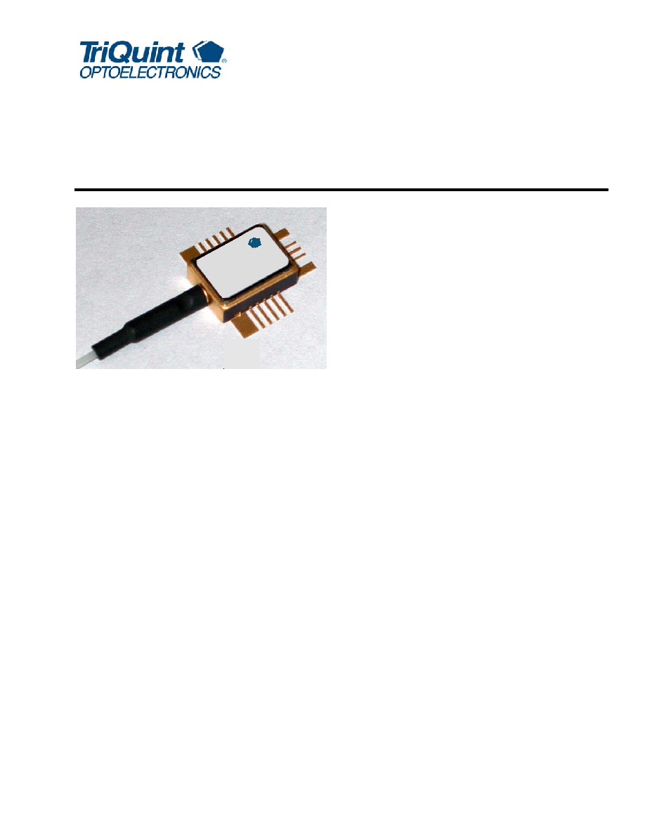
R195P 10 Gb/s Surface-Mount PIN-TIA Receiver
Preliminary Data Sheet, Rev. 1.0
October 2003
Features
Up to 10.7 Gb/s data-rate capability
≠19 dBm typical sensitivity
3 dBm overload typical
2000
typical differential gain
Flat group delay
Very small, surface-mount form factor
Applications
WDM
SONET transponders
Very dense line cards
Description
The R195P receiver integrates a 10 Gb/s PIN and TIA
into a true surface-mount package. It is part of the
industry's first multisource agreement (MSA) to stan-
dardize surface-mount 10 Gb/s receivers. These com-
pact receivers can be mounted directly to a printed-
circuit board, thus avoiding the space, routing, and EMI
problems of a mechanical cut-out.
The R195P provides features optimized for WDM
applications, most notably, linearity and flat group
delay.
riQ
T
uint
OP
TO
EL
EC
TR
ON
ICS
Æ
R1
95PC
A

2
For additional information and latest specifications, see our website: www.triquint.com
Preliminary Data Sheet, Rev. 1.0
R195P 10 Gb/s Surface-Mount PIN-TIA Receiver
October 2003
Absolute Maximum Ratings
Stresses in excess of the absolute maximum ratings can cause permanent damage to the device. These are abso-
lute stress ratings only. Functional operation of the device is not implied at these or any other conditions in excess
of those given in the operational sections of the data sheet. Exposure to absolute maximum ratings for extended
periods can adversely affect device reliability.
1. Based on human-body model of R = 1500
and C = 100 pF. In general, ESD precautions should be taken to avoid damage to the device.
Recommended Operating Conditions
Electrostatic Discharge
CAUTION: This device is susceptible to damage as a result of electrostatic discharge. Take proper precau-
tions during both handling and testing. Follow guidelines such as JEDEC Publication No. 108-A
(Dec. 1988).
TriQuint employs a human-body model (HBM) for ESD-susceptibility testing and protection-design evaluation. ESD
voltage thresholds are dependent on the critical parameters used to define the model. A standard HBM (resistance
= 1.5 k
, capacitance = 100 pF) is widely used and can be used for comparison purposes.
Parameter
Symbol
Min
Max
Unit
Storage Case Temperature Range
T
stg
≠40
85
∞C
TIA Supply Voltage
V
EE
≠5.75
0.5
V
Photodiode Bias Voltage
V
PD
GND
12
V
Optical Input Power
P
IN
--
6
dBm
ESD-susceptibility, All Pins
1
--
--
500 V
Table 1. Recommended Operating Conditions
Parameter
Symbol
Min
Typ
Max
Unit
Optical Wavelength
1280
--
1610
nm
Photodiode Bias Voltage
V
PD
3.1
3.3
3.5
V
Operating Case Temperature Range
T
OP
≠5
25
85
∞C
TIA Supply Voltage
V
EE
≠5.5
≠5.2
≠4.95
V

For additional information and latest specifications, see our website: www.triquint.com
3
Preliminary Data Sheet, Rev. 1.0
October 2003
R195P 10 Gb/s Surface-Mount PIN-TIA Receiver
Electrical/Optical Characteristics
Specified characteristics apply for the recommended operating conditions at beginning of life, unless noted other-
wise. Temperatures are case temperature.
1. External modulator T
X
, BW > 10 GHz,
= 1550 nm ± 10 nm, extinction ratio > 12 dB, NRZ (e.g., Agilent
Æ
Model 83433).
2. The resistance of the thermistor is inversely proportional to the temperature. The temperature, in degree-Kelvin (T
K)
, can be calculated from
the resistance value using the Steinhart-Hart equation: 1/T
K
= A + B ln(R) + C [ln(R)]
3
, where R is the resistance and A, B, and C are con-
stants: A = 1.0267 x 10
≠3;
B = 2.565 x 10
≠4
;
C = ≠4.5421 x 10
≠8
.
The temperature, in degree-Celsius, is T
C
= T
K
≠ 273.15.
3. For 25 ∞C, nominal bias voltage and optical input = ≠20 dBm ± 0.2 dB.
Note: Accuracy of optical powers in test condition column is ± 0.2 dB.
Table 2. Electrical/Optical Characteristics
Parameter
Symbol
Condition
Min
Typ
Max
Unit
Sensitivity
1
--
OC-192, PRBS 2
31
≠ 1 NRZ,
BER = 10
≠12
, 25 ∞C
--
≠19.0
≠18.0
dBm
Overload
1
--
OC-192, PRBS 2
31
≠ 1 NRZ,
BER = 10
≠12
, 25 ∞C
1
3
--
dBm
Responsivity,
= 1550 nm
R
25 ∞C Case
≠5 ∞C to +85 ∞C Case
0.75
0.7
0.85
0.8
--
--
A/W
Dark Current
I
D
25 ∞C Case
--
--
1
nA
Thermistor Resistance
2
R
TH
25 ∞C
9.5
10.0
10.5
k
Thermistor Temperature Coef-
ficient
--
--
--
≠4.3
--
%/∞C
Transimpedance
3
Z
T
Small Signal, Differential
1.6
2.0
2.4
k
Small Signal Bandwidth
3
S
21
--
7.5
9.5
--
GHz
Low-frequency cutoff
--
P
IN
= ≠20 dBm
≠3 dB relative to 1 MHz
--
25
40
KHz
Output Return Loss
3
S
22
50
on each output
0.2 GHz--8 GHz
--
--
≠8
dB
Group Delay
2
GD
0.5 GHz--5 GHz
5 GHz--8 GHz
--
--
--
--
±25
±40
ps,p-p
ps,p-p
TIA Supply Current
I
EE
≠5 ∞C to +85 ∞C
--
130
155
mA
Output Voltage
Vout
Single-ended, 50
load
--
700
1000
mVp-p
Optical Return Loss
RL
1300 nm--1610 nm;
without connector
27
--
--
dB

4
For additional information and latest specifications, see our website: www.triquint.com
Preliminary Data Sheet, Rev. 1.0
R195P 10 Gb/s Surface-Mount PIN-TIA Receiver
October 2003
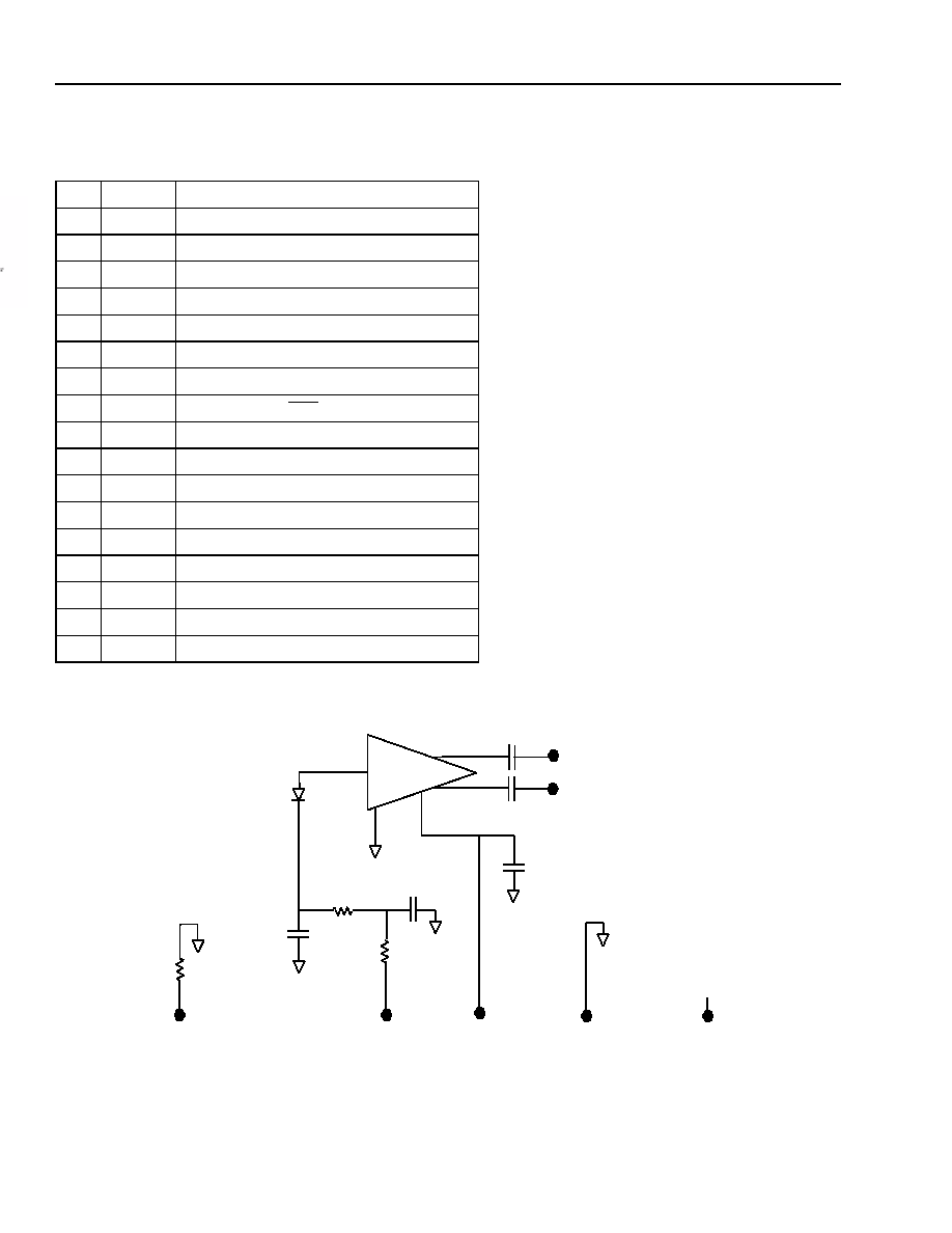
Pin Information
Block Diagram
Table 3. Pin Information
Pin
Symbol
Function
1
GND
Case Ground
2
V
PD
Photodiode Bias
3
NC
No Connection
4
V
EE
TIA Bias (≠5.2 V)
5
NC
No Connection
6
GND
Case Ground
7
GND
Case Ground
8
Out
_
N
Data
Output
9
GND
Case Ground
10
Out
_
P
Data Output
11
GND
Case Ground
12
GND
Case Ground
13
NC
No Connection
14
NC
No Connection
15
NC
No Connection
16
R
TH
Thermistor
17
GND
Case Ground
Pin 16
Thermistor
Pin 2
V
PD
Pin 4
V
EE
Pin 1,6,7,9,11,12,17
GND
Pin 3,5,13,14,15
No Connection
Pin 8
OUT_N
Pin 10
OUT_P
Transim.
Amp.
Photodetector
Pin 16
Thermistor
Pin 2
V
PD
V
Pin 1,6,7,9,11,12,17
GND
No Connection
Pin 8
OUT_N
Pin 10
OUT_P
Transim.
Amp.
PIN
Photodetector
Pin 16
Thermistor
Pin 2
V
PD
Pin 4
V
EE
Pin 1,6,7,9,11,12,17
GND
Pin 3,5,13,14,15
No Connection
Pin 8
OUT_N
Pin 10
OUT_P
Transim.
Amp.
Photodetector
Pin 16
Thermistor
Pin 2
V
PD
V
Pin 1,6,7,9,11,12,17
GND
No Connection
Pin 8
OUT_N
Pin 10
OUT_P
Transim.
Amp.
PIN
Photodetector

For additional information and latest specifications, see our website: www.triquint.com
5
Preliminary Data Sheet, Rev. 1.0
October 2003
R195P 10 Gb/s Surface-Mount PIN-TIA Receiver
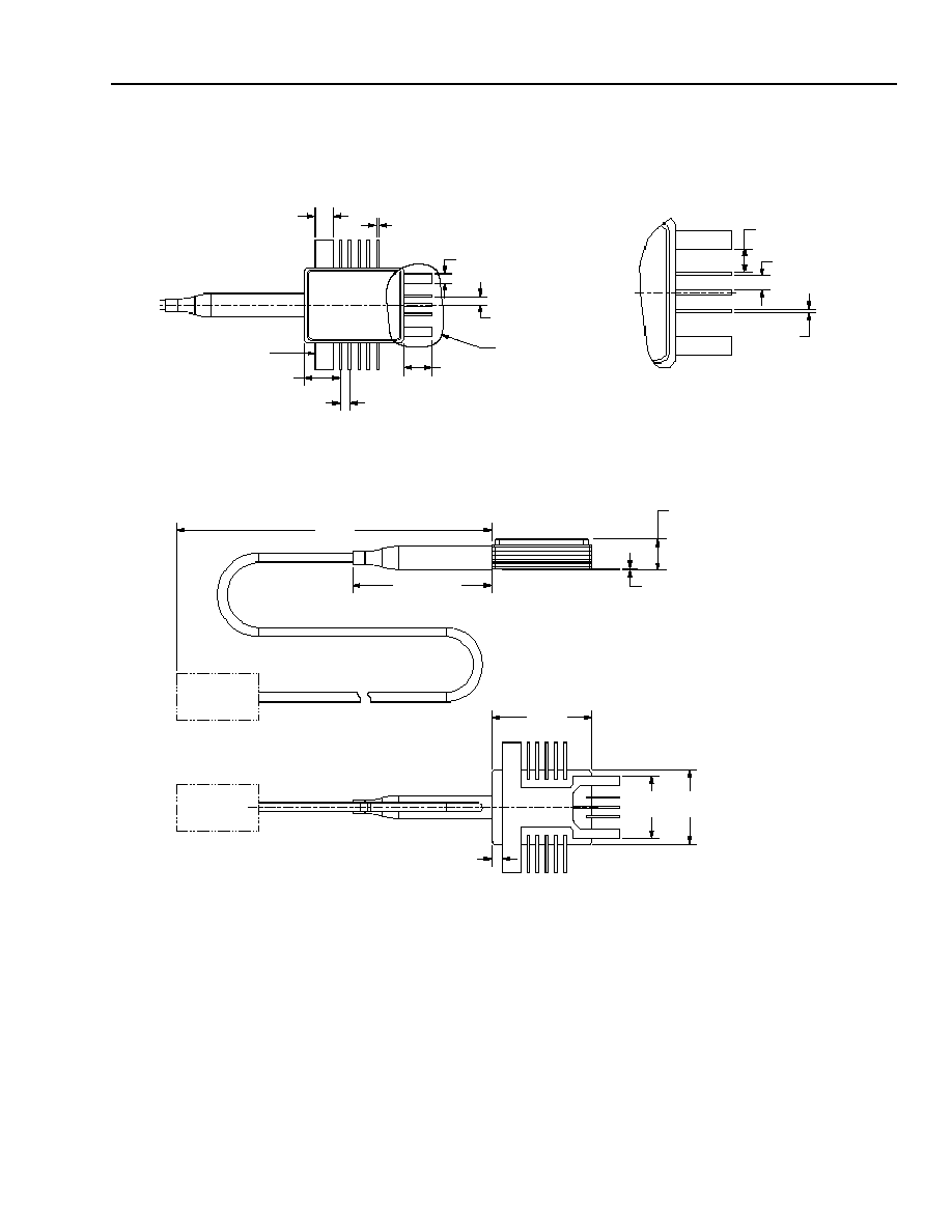
Outline Diagram
Dimensions are in inches and (millimeters).
0.079
(2.00)
11X 0.012
(0.30)
2X 0.039
(1.00)
0.035
(0.90)
SEE DETAIL A
0.118 TYP
(3.00)
0.153
(3.90)
0.039 TYP
(1.00)
0.049
(1.25)
0.030
(0.75)
2X 0.008
(0.20)
DETAIL A
SCALE 8.000
DIM A
0.13
(3.3)
0.008
(0.20)
20 mm MAX
0.423
(10.75)
0.315
(8.00)
0.04
(1.1)
0.264
(6.70)
PIN 1

Additional Information
For the latest specifications, additional product information, worldwide sales and distribution locations, and information about TriQuint:
Web: www.triquint.com
Tel: (484) 397-3800
E-mail: info_opto@tqs.com
Fax: (484) 397-3592
For technical questions and additional information on specific applications:
E-mail: info_opto@tqs.com
The information provided herein is believed to be reliable; TriQuint assumes no liability for inaccuracies or omissions. TriQuint assumes no responsibility for the use of this information, and all
such information shall be entirely at the user's own risk. Prices and specifications are subject to change without notice. No patent rights or licenses to any of the circuits described herein are
implied or granted to any third party.
TriQuint does not authorize or warranty any TriQuint product for use in life-support devices and/or systems.
Copyright © 2003 TriQuint Semiconductor Inc. All rights reserved.
DS03-043-1 Rev. 1.0, October 2003 (Replaces DS03-043)
Preliminary Data Sheet, Rev. 1.0
R195P 10 Gb/s Surface-Mount PIN-TIA Receiver
October 2003
Ordering Information
Table 4. R195P-Type Receiver Ordering Information
Product Code
Detector Type
Connector type
Fiber type
R195PCA
PIN
SC/PC
SMF
R195PCF
PIN
FC/PC
SMF
R195PCS
PIN
LC
SMF
R195PCJ
PIN
MU
SMF
R195PCJJ
PIN
MU-J
SMF
Agilent is a registered trademark of Agilent Technologies, Inc.
