 | –≠–ª–µ–∫—Ç—Ä–æ–Ω–Ω—ã–π –∫–æ–º–ø–æ–Ω–µ–Ω—Ç: RA192 | –°–∫–∞—á–∞—Ç—å:  PDF PDF  ZIP ZIP |

RA192 OC-192/STM-64 APD Lightwave Receiver
Preliminary Data Sheet
February 2003
TriQuint Optoelectronics
Featuring improved sensitivity for optimum performance in
noisy, amplified systems, the RA192 Receiver is manufactured
in a compact, 16-pin butterfly package (above), and is also avail-
able with a convenient mounting bracket (below).
Features
High data rate capability, 10 Gb/s
APD photodetector
Fully operational through the 1.3
µm to 1.6 µm wave-
length range
Typical sensitivity of ≠26 dBm, overload of ≠2 dBm
Excellent group-delay performance for DWDM appli-
cations
Single-mode fiber pigtail with SC, FC, LC, or
MU optical connector
Operating case temperature range:
0 ∞C to 70 ∞C
50
differential data output, with offset control
Package options:
-- Space-sensitive package without mounting
bracket (ideal for transponder and transceiver
applications)
-- With mounting bracket
Applications
Line terminal equipment
High-speed networks up to 10 Gb/s
SONET/SDH OC-192/STM-64 telecommunications
applications
Extended-reach datacom and telecom applications
Æ
riQ
T
uint
SEMICON
DUCTOR
RA192
RA19
2
Æ
riQ
T
uint
SEM
ICON
DUCT
OR
2
2
For additional information and latest specifications, see our website: www.triquint.com
Preliminary Data Sheet
RA192 OC-192/STM-64 APD Lightwave Receiver
February 2003
Description
Receiver Operation
The RA192 10 Gb/s fiber-optic receiver consists of a
high-speed APD photodetector and a wide-band linear
preamp in a pigtailed, butterfly metal package. The
fiber pigtail is internally beveled for low return loss and
is available with SC, FC, LC, or MU optical connectors.
It is designed for use in single-mode, high-speed tele-
communication applications at the SONET OC-192
and the ITU-T SDH STM-64 data rate of 9.95328 Gb/s.
At 9.95328 Gb/s, the typical room temperature sensitiv-
ity at a BER of 1 x 10
≠10
is ≠26 dBm, and the typical
room temperature overload at a BER of 1 x 10
≠10
is
≠2 dBm. The operating case temperature range for the
receiver is 0 ∞C to 70 ∞C.
The dc levels of the differential outputs can be adjusted
relative to each other for optimum sensitivity in noisy,
amplified systems. These outputs are centered around
a dc level of typically ≠0.45 V when the two outputs are
dc-coupled to 50
loads. The two outputs can also be
ac coupled. If slice level control is not needed, the FB
IN
pin (pin 14) should be left open. The TIA requires only
a ≠5.2 V power supply for operation. The APD photo-
diode requires a nominal bias voltage of 25 V to 36 V at
less than 1 mA.
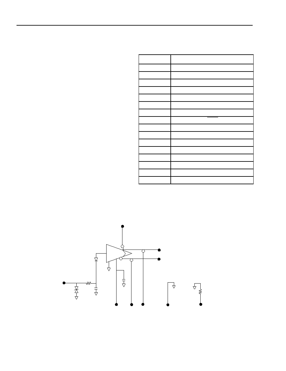
Pin Information
Table 1. Pin Descriptions
Pin Number
Name
1
APD Bias
2
GND
3
V
EE
4
NC
5
NC
6
NC
7
GND
8
DATA
9
DATA
10
GND
11
NC
12
≠OFF
13
+OFF
14
Feedback Input Threshold Control
15
GND
16
Thermistor
Electrical Schematic
Figure 1. Electrical Schematic
T
Z
AMP
APD
PIN 1
PIN 3 PIN 12 PIN 13
V
EE
≠OFF
+OFF
PIN 2, 7, 10, 15,
GND
PIN 16
THERMISTOR
V
PD
PIN 14
FB
IN
PIN 9
OUT_P
PIN 8
OUT_N
PHOTODIODE

For additional information and latest specifications, see our website: www.triquint.com
3
Preliminary Data Sheet
February 2003
RA192 OC-192/STM-64 APD Lightwave Receiver
Absolute Maximum Ratings
Stresses in excess of the absolute maximum ratings can cause permanent damage to the device. These are abso-
lute stress ratings only. Functional operation of the device is not implied at these or any other conditions in excess
of those given in the operations section of the data sheet. Exposure to absolute maximum ratings for extended
periods can adversely affect device reliability.
* Device is normally reverse biased. Forward biasing the photodiode can compromise device performance and reliability.
Optical Characteristics
Parameter
Symbol
Min
Max
Unit
Supply Voltages:
Negative Supply
V
EE
≠4.7
≠5.7
V
Photodiode Supply Current:
Forward*
Reverse
--
--
--
--
TBD
TBD
mA
mA
APD Bias Voltage
V
APD
GND
V
BR
V
Optical Input Power (biased)
P
MAX
--
0
dBm
Operating Case Temperature Range
T
C
0
70
∞C
Storage Temperature Range
T
stg
≠40
85
∞C
Lead Soldering Temperature
--
--
250
∞C
Lead Soldering Time
--
--
10
s
Table 2. Optical Characteristics (T
C
= 25 ∞C,
= 1550 nm, V
EE
= ≠5.2 V unless otherwise specified)
Parameter
Symbol
Min
Typ
Max
Unit
Optical Wavelength
1.3
--
1.61
µm
Sensitivity (9.953 Gb/s, 2
31
≠ 1 PRBS, 1 x 10
≠10
BER,
ER = 12 dB, NRZ, V
APD
= V
OP
):
25 ∞C
0 ∞C to 70∞C
P
LOW
--
--
≠26.0
≠25.5
≠25.5
≠25.0
dBm
dBm
Overload (9.953 Gb/s, 2
31
≠ 1 PRBS, 1 x 10
≠10
BER,
ER = 12 dB, NRZ):
25 ∞C
0 ∞C to 70∞C
P
HIGH
≠2
≠3
--
--
--
--
dBm
dBm
Optical Return Loss
RL
--
--
≠27
dB
Responsivity (M = 1):
= 1.55 µm
= 1.3 to 1.61 µm
R
0.65
0.59
0.8
--
--
--
A/W
A/W
Total Dark Current (V
APD
= V
OP
)
I
D
--
100
200
nA

4
For additional information and latest specifications, see our website: www.triquint.com
Preliminary Data Sheet
RA192 OC-192/STM-64 APD Lightwave Receiver
February 2003
Electrical Characteristics
Table 3. Electrical Characteristics (T
C
= 25 ∞C,
= 1550 nm, V
EE
= ≠5.2 V unless otherwise specified)
Parameter
Symbol
Min
Typ
Max
Unit
dc Power Supply Voltages:
Negative Supply
V
EE
≠4.94
≠5.2
≠5.46
V
dc Power Supply Currents:
Negative Supply
I
EE
--
140
155
mA
Power Dissipation
P
DISS
--
--
0.85
W
APD Bias Voltage
1
:
25 ∞C
0 ∞C to 70 ∞C
1. APD optimum bias voltage (V
OP
) differs from device to device and is provided with each device.
V
OP
25
22
33
--
40
44
V
APD Breakdown Voltage:
25 ∞C
0 ∞C to 70 ∞C
V
BR
28
25
--
--
43
47
V
Temperature Coefficient of V
OP
and V
BR
0.05
0.06
0.07
V/∞C
Thermistor Resistance at 25 ∞C
2
2. The resistance of the thermistor is inversely proportional to the temperature. The temperature can be calculated from the resistance value
using the Steinhart-Hart equation: 1/T = A + B ln(R) + C ln(R)
3
;
where T is the temperature in Kelvin degrees, R is the thermistor resistance
value in Ohms, and A, B, and C are constants: A = 1.0267 x 10
≠3,
B = 2.565 x 10
≠4
,
C = - 4.5421 x 10
≠8
.
R
TH
9.5
10
10.5
k
Transimpedance (Single-ended, ≠26 dBm optical
input power)
Z
T
1
1.4
1.8
k
Output Voltage (Single-ended, V
APD
= V
OP
,
9.953 Gb/s, ≠26 dBm)
V
SENS
--
40
--
mVp-p
Output Voltage (Single-ended, V
APD
= V
OP
,
9.953 Gb/s, ≠2 dBm)
V
OVERLOAD
600
800
1000
mVp-p
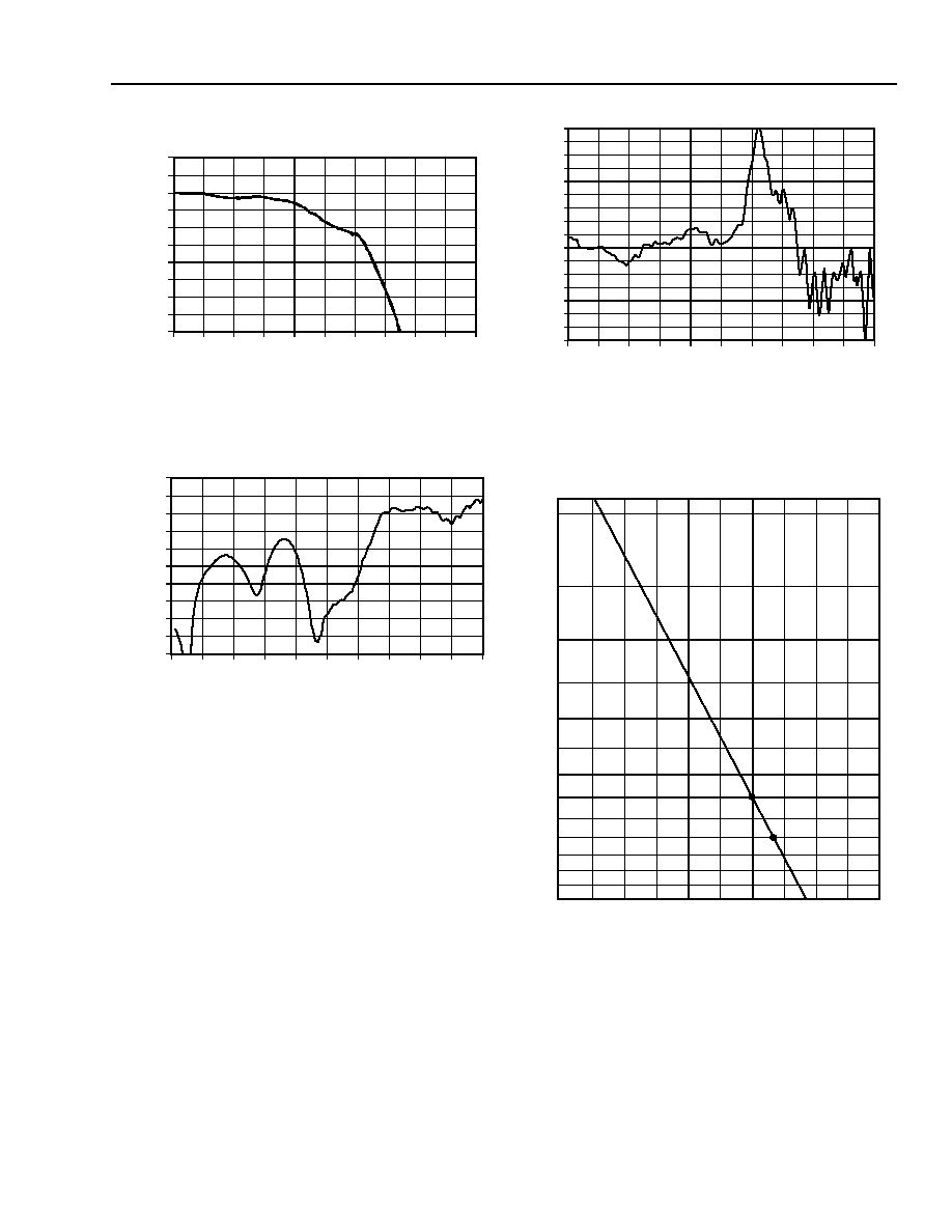
3 dB Bandwidth (V
APD
= V
OP
, ≠20 dBm)
BW
8.0
8.8
--
GHz
Peaking (0.13 GHz--10 GHz, V
APD
= V
OP
, ≠20 dBm)
--
--
0
1
dB
Group Delay Deviation (0.13 GHz--10 GHz,
V
APD
= V
OP
, ≠20 dBm)
GD
--
--
50
ps
p-p
Output Return Loss (0.13 GHz--10 GHz,
V
APD
= V
OP
, ≠20 dBm)
S
22
--
≠14
≠9
dB
Preliminary Data Sheet
February 2003
RA192 OC-192/STM-64 APD Lightwave Re-
For additional information and latest specifications, see our website: www.triquint.com
5
Characteristic Curves
Figure 2. RA192 Typical Transfer Function
Figure 3. RA192 Typical Output Return Loss
Figure 4. RA192 Typical Group Delay
Deviation (5% Smoothing)
Figure 5. RA192 Typical BER CURVE
6
3
0
≠3
≠6
≠9
≠12
≠15
≠18
≠21
GAIN (dB)
FREQUENCY (GHz)
0
2
4
6
8
10
12
14
16
18
20
≠24
0
≠3
≠6
≠9
≠12
≠15
≠18
≠21
≠24
≠27
OUTPUT MATCH
(db)
FREQUENCY (GHz)
0
2
4
6
8
10
12
14
16
18
20
≠30
80
70
60
50
40
30
20
10
0
≠10
≠20
≠30
≠40
≠50
≠60
≠70
≠80
GO
OUP DELAY (P
S)
0
2
4
6
8
10
12
14
16
18
20
FREQUENCY (GHz)
1
≠3
1
≠4
1
≠5
1
≠7
1
≠8
1
≠9
1
≠10
1
≠11
1
≠12
1
≠13
1
≠14
1
≠15
≠32
≠30
≠28
≠26
≠24
≠22
OPTICAL POWER (dBm)
1
≠16
1
≠6
6
6
For additional information and latest specifications, see our website: www.triquint.com
Preliminary Data Sheet
RA192 OC-192/STM-64 APD Lightwave Receiver
February 2003
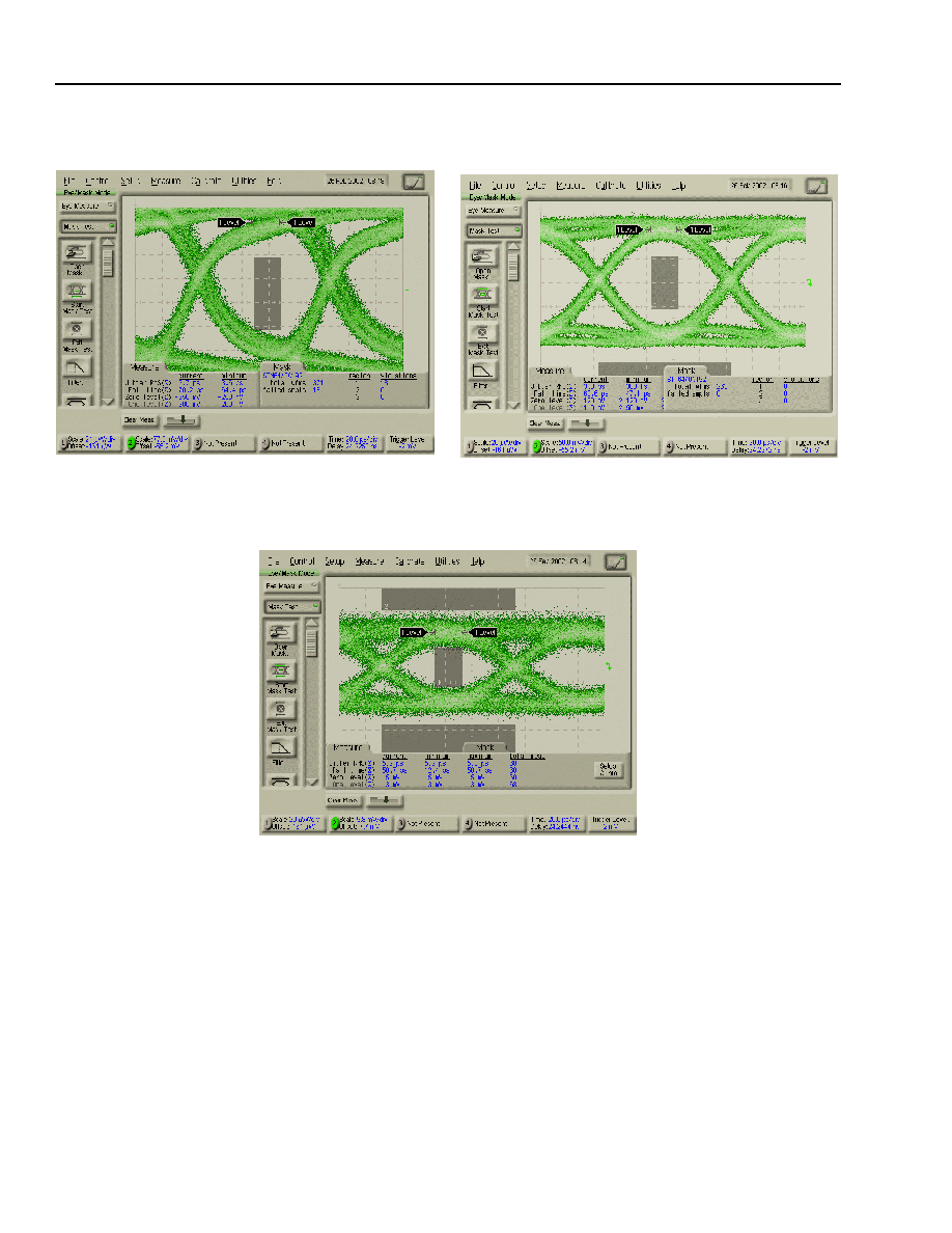
Characteristic Curves
(continued)
Figure 6. RA192 Eye Pattern at ≠1.4 dBm
Input Power
Figure 7. RA192 Eye Pattern at ≠15 dBm
Input Power
Figure 8. RA192 Eye Pattern at ≠26.2 dBm Input Power

For additional information and latest specifications, see our website: www.triquint.com
7
Preliminary Data Sheet
February 2003
RA192 OC-192/STM-64 APD Lightwave Receiver
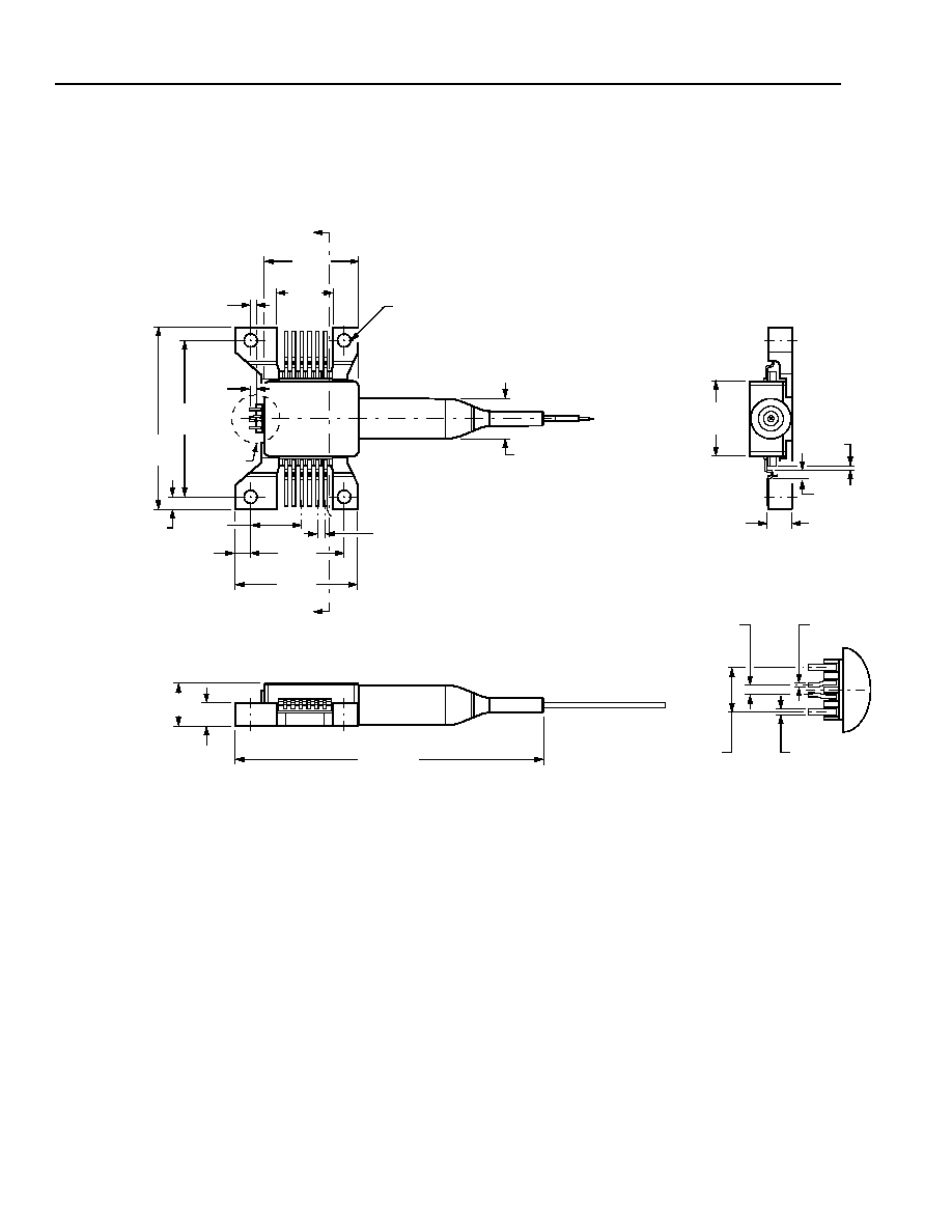
Outline Diagrams
Outline Drawing, Package Style N
Dimensions are in inches and (millimeters).
1
6
0.170
(4.32)
0.050
(1.27)
0.175
(4.44)
0.500
(12.70)
7
10
11
16
0.260
(6.60)
0.500
(12.70)
0.150
(3.80)
0.043
(1.10)
0.042
(1.10)
SECTION A-A
0.146
(3.70)
0.272
(6.90)
A
0.060
(1.52)
0.156
(3.95)
0.606
(15.38)
0.087
(2.22)
A
0.020
(0.51)
0.050
(1.27)
0.569
(14.45)
1.135
(28.84)
0.354
(9.00)
0.611
(15.51)
0.004
(0.100)
0.037
(0.95)
0.354
(9.00)
0.611
(15.51)
0.157
(4.00)
0.276
(7.00)
2 x 0.008
(0.20)
2 x 0.016
(0.40)
0.013
(0.32)
0.025
(0.64)
0.063
(1.59)
0.125
(3.18)
0.315
8.00)
1-1236
8
For additional information and latest specifications, see our website: www.triquint.com
Preliminary Data Sheet
RA192 OC-192/STM-64 APD Lightwave Receiver
February 2003
Outline Diagrams
(continued)
Outline Drawing, Package Style A
Dimensions are in inches and (millimeters).
1
6
0.375
(9.53)
0.611
(15.51)
0.037
(0.95)
0.050
(1.27)
1.017
(25.83)
1.174
(29.82)
7
10
11
16
DETAIL "B"
4 x 0.087(2.20)
0.333
(8.45)
0.050
(1.27)
0.608
(15.45)
0.797
(20.25)
0.097
(2.46)
0.260
(6.60)
0.500
(12.70)
0.150
(3.80)
0.043
(1.10)
0.042
(1.10)
SECTION A≠A
0.150
(3.80)
0.272
(6.90)
2.010 REF.
(51.05)
DETAIL B
0.016
(0.40)
0.008
(0.20)
0.025
(0.64)
0.125
(3.18)
A
A
0.079
(2.00)
1-1237

Additional Information
For the latest specifications, additional product information, worldwide sales and distribution locations, and information about TriQuint:
Web: www.triquint.com
Tel: (503) 615-9000
E-mail: info_opto@tqs.com
Fax: (503) 615-8902
For technical questions and additional information on specific applications:
E-mail: info_opto@tqs.com
The information provided herein is believed to be reliable; TriQuint assumes no liability for inaccuracies or omissions. TriQuint assumes no responsibility for the use of this information, and all
such information shall be entirely at the user's own risk. Prices and specifications are subject to change without notice. No patent rights or licenses to any of the circuits described herein are
implied or granted to any third party.
TriQuint does not authorize or warranty any TriQuint product for use in life-support devices and/or systems.
Copyright © 2003 TriQuint Semiconductor Inc. All rights reserved.
DS02-185 Revision 1.1, February, 2003
Preliminary Data Sheet
RA192 OC-192/STM-64 APD Lightwave Receiver
February 2003
Electrostatic Discharge
CAUTION: This device is susceptible to damage as a result of electrostatic discharge. Take proper precau-
tions during both handling and testing. Follow guidelines such as EIA
Æ
Standard EIA 625.
TriQuint Semiconductor employs a human-body model (HBM) for ESD-susceptibility testing and protection-design
evaluation. ESD voltage thresholds are dependent on the critical parameters used to define the model. A standard
HBM (resistance = 1.5 k
, capacitance = 100 pF) is widely used and can be used for comparison purposes.
Ordering Information
Table
4. Ordering Information
Description
Product Code
Package Style
Connector
Comcode
RA192-Type OC-192/STM-64 APD
Lightwave Receiver
RA192WDAA A
SC
700022259
RA192WGAA
A
FC
700022260
RA192WSAA
A
LC
700022261
RA192WYAA
A
MU
700022262
RA192WDAN
N
SC
700022263
RA192WGAN
N
FC
700022264
RA192WSAN
N
LC
700022265
RA192WYAN
N
MU
700022266
EIA is a registered trademark of Electronic Industries Association.