 | –≠–ª–µ–∫—Ç—Ä–æ–Ω–Ω—ã–π –∫–æ–º–ø–æ–Ω–µ–Ω—Ç: T923JFAA | –°–∫–∞—á–∞—Ç—å:  PDF PDF  ZIP ZIP |

T92-Type 10 Gb/s 1300 nm
Uncooled DFB Laser Transmitter
Data Sheet
March 2003
Offering SONET/SDH compatibility, the T92-Type Uncooled
Laser Transmitter is manufactured in a 24-pin DIP assembly
with a single-mode fiber pigtail.
Features
MSA compliant, 24-pin package
Data rates from 9.95 Gb/s to 10.7 Gb/s
SDH STM-64 VSR600-2R1 and VSR2000-2R1
compliant
Transmission distances up to 40 km
Uncooled, InGaAsP MQW laser
1300 nm DFB
Nonlocked operation with single-ended or differen-
tial inputs
50
ac-coupled 600 mVp-p--1000 mVp-p single-
ended data
Operation from single ≠5.2 V or +5.0 V power sup-
ply
Automatic optical power control
Wide operating case temperature range: 0 ∞C to
70 ∞C
Laser bias monitor output
riQ
T
ui
nt
Æ
O
PT
O
EL
EC
TR
O
N
IC
S,
IN
C
.
T9
2
Tr
an
sm
itt
er
Normalized laser back-facet monitor output
Laser degrade alarm
Transmitter disable input
SC, FC-PC, LC, and MU optical connector options
Applications
Telecommunications:
-- SONET/SDH
-- Subscriber loop
-- Metropolitan area networks
High-speed data communications
-- 10G Ethernet
-- 10G Fibre Channel
Description
The T92-Type 10 Gb/s laser transmitters are
designed for use in transmission systems and high-
speed data communication applications. For trans-
mission system applications, the transmitter oper-
ates at the SONET OC-192 standard and FEC rates,
and SDH rate of STM-64 standard and FEC rates as
per ITU-T G.709. For high-speed data communica-
tions, the transmitter operates at 10G Ethernet rate
and 10G Fibre Channel rate.
The transmitters meet all present Telcordia Technol-
ogies
TM GR-253-CORE requirements and the ITU-T
G.693 recommendations. The transmitters are also
ideally suited for extended distance data and net-
working applications.
Manufactured in a 24-pin DIP assembly, the trans-
mitter uses an hermetic, isolated, 1300 nm MQW
DFB laser, an InGaAs PIN photodiode back-facet
monitor and a GaAs laser driver IC. The transmitter
requires a single power supply (≠5.2 V or +5.0 V).
Pin information is listed in Table 1.

T92-Type 10 Gb/s 1300 nm
Data Sheet
Uncooled DFB Laser Transmitter
March 2003
2
2
For additional information and latest specifications, see our website: www.triquint.com
Description
(continued)
Transmitter Processing
The transmitter can withstand normal wave soldering
processes. The complete transmitter module is not her-
metically sealed; therefore, it should not be immersed
in or sprayed with any cleaning solution or solvents.
The process cap and fiber pigtail jacket can deform at
temperatures greater than 85 ∞C. The transmitter pins
can be wave-soldered at a maximum temperature of
250 ∞C for 10 seconds.
Installation Considerations
Although the transmitter has been designed with rug-
gedness in mind, care should be used during handling.
The optical connector should be kept free from dust,
and the process cap should be kept in place as a dust
cover when the device is not connected to a cable. If
contamination is present on the optical connector, the
use of canned air with an extension tube should
remove any debris. Other cleaning procedures are
identified in the Cleaning Fiber-Optic Assemblies Tech-
nical Note (TN95-010).
Laser Degrade-Mode Alarm
An output of the transmitter that indicates when the
laser bias has reached its end-of-life condition. The
transmitter will still function, but may not meet all speci-
fications. The transmitter should be replaced when this
alarm is active (active-low). Specifically, this alarm indi-
cates that the bias of the laser has changed more than
50% from its original value.
Back-facet Monitor Output
This is an analog output that indicates whether the
transmitter has the correct optically generated back-
facet current. It may be used for alarm purposes. It is
referenced to V
EE
. Under normal operating conditions,
this monitor will output a voltage that is nominally
500 mV above V
EE
. When the optical output power of
the transmitter increases or decreases, this voltage will
move proportionately.
Bias Monitor Output
This is an analog output voltage that indicates the bias
current being supplied to the laser. It is referenced to
V
EE
. The conversion for this monitor output is 20 mV
for every 1 mA of bias current to the laser. For exam-
ple, a 400 mV output above V
EE
would indicate 20 mA
of bias current to the laser.
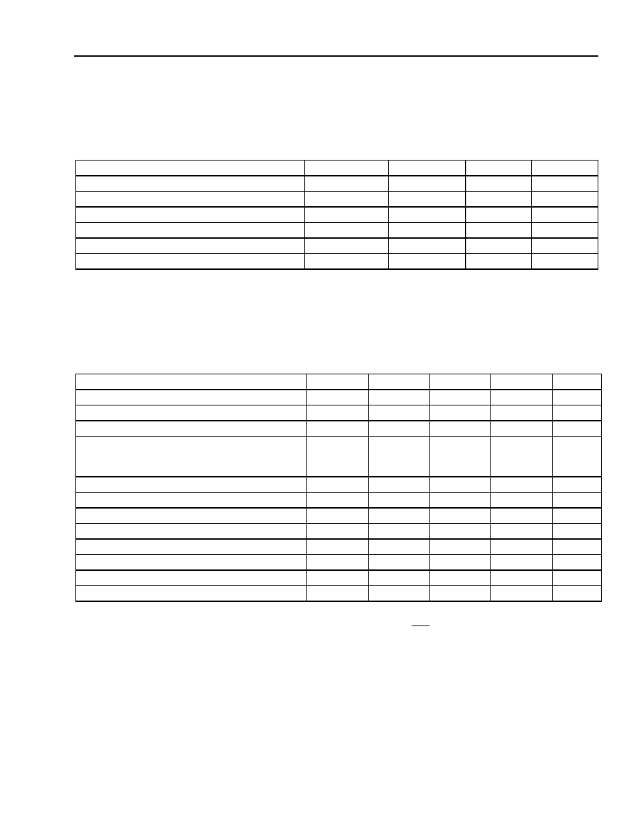
Table 1. Pin Descriptions
1. Laser back-facet function is a customer-use option that is not
required for normal operations of the transmitter and is normally
used during manufacture and for diagnostics.
2. Laser temperature (∞C) = (V
TEMP
≠ 0.5 V)/0.01 V, where V
TEMP
is
the temperature monitor voltage.
3. This pin can be tied to ground.
4. For single-ended operation, data signal must be on pin 16, and
DATA
(pin 18) must 50
terminated to ground.
NUC = No user connection. Pin must not be tied to ground or any
other circuit potential.
Pin Number
Name
1
V
EE
2
Back-facet Monitor
1
3
Bias Monitor
4
Tx Enable
5
NUC
6
Ground
7
Temperature Monitor
2
8
Laser Degrade Alarm
9
NUC
10
NUC
11
NUC
3
12
V
EE
13
V
CC
14
NUC
15
Ground
16
DATA
4
17
Ground
18
DATA
4
19
Ground
20
NUC
21
Ground
22
NUC
23
Ground
24
V
CC
Data Sheet
T92-Type 10 Gb/s 1300 nm
March 2003
Uncooled DFB Laser Transmitter
3
For additional information and latest specifications, see our website: www.triquint.com
Absolute Maximum Ratings
Stresses in excess of the absolute maximum ratings can cause permanent damage to the device. These are abso-
lute stress ratings only. Functional operation of the device is not implied at these or any other conditions in excess
of those given in the operations sections of the data sheet. Exposure to absolute maximum ratings for extended
periods can adversely affect device reliability.
Characteristics
(Minimum and maximum values specified over operating case temperature range at 50% duty cycle data signal.
Typical values are measured at room temperature unless otherwise noted.)
1. With V
EE
connected to ≠5.2 V, V
CC
must be at 0 V; With V
CC
connected to +5.0 V, V
EE
must be at 0 V.
2. Inputs are ac-coupled into an equivalent input impedance of 50
.
3. Single-ended or differential operation may be used. If the inputs are driven single-ended, Data must be 50
terminated to ground.
4. The transmitter is normally enabled and requires an external voltage to disable.
5. This alarm will go active when the bias current to the laser has increased 50% or more from its beginning-of-life (BOL) value.
6. This voltage is measured from Pin 3 to V
EE
and is converted to laser bias current with the ratio of 20 mV/mA.
7. This voltage is measured from Pin 2 to V
EE
.
Parameter
Symbol
Min
Max
Unit
Supply Voltage
V
CC
--
5.5
V
Operating Case Temperature Range
T
C
0
70
∞C
Storage Case Temperature Range
T
stg
≠40
85
∞C
Lead Soldering Temperature/Time
--
--
250/10
∞C/s
Relative Humidity (noncondensing)
RH
--
85
%
Minimum Fiber-Bend Radius
--
1.00 (25.4)
--
in. (mm)
Table 2. Electrical Characteristics
Parameter
Symbol
Min
Typ
Max
Unit
Bit Rate
--
9.953
--
10.709
Gb/s
dc Power Supply Voltage
1
V
EE
≠5.5/+4.75
≠5.2/+5.0
≠4.9/+5.25
V
dc Power Supply Current Drain
I
--
250
400
mA
Input Data:
2,3
Single-ended Input
Differential Input
V
IN
600
300
700
350
1000
500
mVp-p
mVp-p
Data Input Impedance
R
IN
--
50
--
Data RF Return Loss (50 kHz to 8 GHz)
S11
--
--
≠10
dB
Transmitter Disable Voltage
4
V
DIS
V
CC
≠ 2.0
--
V
CC
V
Transmitter Enable Voltage
V
EN
V
EE
--
V
EE
+ 0.8
V
Degrade Mode Alarm Voltage≠Normal
V
NORMAL
V
CC
≠ 2.0
--
V
CC
V
Degrade Mode Alarm Voltage≠Alarmed
5
V
ALARMED
V
EE
--
V
EE
+ 0.8
V
Laser Bias Voltage
6
V
B
0
500
2400
mV
Back-facet Monitor Voltage (50% duty cycle)
7
V
BF
460
500
540
mV

T92-Type 10 Gb/s 1300 nm
Data Sheet
Uncooled DFB Laser Transmitter
March 2003
4
For additional information and latest specifications, see our website: www.triquint.com
Characteristics
(continued)
1. Output power definitions and measurements per proposals to the ITU-T Recommendation G.693.
2. Full spectral width measured 20 dB down from the maximum of the central wavelength peak under fully modulated conditions.
3. Ratio of the peak output power in the dominant longitudinal mode to the power in the most significant side mode under fully modulated condi-
tions.
4. Ratio of logic 1 output power to logic 0 output under fully modulated conditions.
Table 3. Optical Characteristics
Parameter
Symbol
Min
Typ
Max
Unit
Average Power Output, T923xFAA
1
P
O
≠6 ≠2 ≠1
dBm
Center Wavelength Range, T923xFAA
C
1290
--
1330
nm
Spectral Width
2
20
--
--
1
nm
Wavelength Shift with Temperature
/
T
--
0.1
--
nm/∞C
Side-mode Suppression Ratio
3
SMSR
30
--
--
dB
Optical Return Loss
S
22
30
--
--
dB
Optical Isolation
I
S
20
--
--
dB
Dispersion Penalty (12 km max, G.652)
D
P
--
--
1
dB
Extinction Ratio
4
r
e
6
7
--
dB
Eye Mask of Optical Output
--
per GR-253 CORE
and ITU G.693 and G.709
--

Data Sheet
T92-Type 10 Gb/s 1300 nm
March 2003
Uncooled DFB Laser Transmitter
5
For additional information and latest specifications, see our website: www.triquint.com
Outline Drawings
Dimensions are in inches and (millimeters).
1.450
(36.83)
2.015
(51.18)
1.055
(26.80)
0.260
(6.60)
0.392
(9.96)
0.100 ± 0.01
(2.54 ± 0.254)
0.100
(2.54)
0.018
(0.46)
0.015
(0.38)
1.100
(27.94)
0.720
(18.29)
1.000
(25.40)
1-1256(F)
{

T92-Type 10 Gb/s 1300 nm
Data Sheet
Uncooled DFB Laser Transmitter
March 2003
6
For additional information and latest specifications, see our website: www.triquint.com
Qualification and Reliability
To help ensure high product reliability and customer satisfaction, TriQuint is committed to an intensive quality pro-
gram that starts in the design phase and proceeds through the manufacturing process. Optoelectronics modules
are qualified to TriQuint's internal standards using MIL-STD-883 test methods and procedures and using sampling
techniques consistent with Telcordia Technologies requirements. This qualification program fully meets the intent of
Telcordia GR-468-CORE reliability practices. In addition, the TriQuint design, development, and manufacturing
facility has been certified to be in full compliance with ISO
Æ
9001 Quality System Standards.
Electrostatic Discharge
CAUTION: This device is susceptible to damage as a result of electrostatic discharge. Take proper precau-
tions during both handling and testing. Follow guidelines such as JEDEC Publication No. 108-A
(Dec. 1988).
TriQuint employs a human-body model (HBM) for ESD-susceptibility testing and protection-design evaluation. ESD
voltage thresholds are dependent on the critical parameters used to define the model. A standard HBM (resistance
= 1.5 k
, capacitance = 100 pF) is widely used and can be used for comparison purposes. The HBM ESD with-
stand voltage established for the T923-type transmitter is 100 V.
Laser Safety Information
Class I Laser Product
All versions of the T92-type transmitters are classified as Class I laser products per FDA/CDRH, 21 CFR 1040
Laser Safety requirements. The transmitters are classified with the FDA under accession number 8720009. All ver-
sions are classified as Class I laser products per IEC
Æ
60825-1:1993.
This product complies with 21 CFR 1040.10 and 1040.11.
Wavelength = 1300 nm
Maximum power = 10 mW
Connector Options
The standard optical fiber pigtail is 8
µm core single-mode fiber having a 0.036 in. (914 mm) diameter tight-buffered
outer-jacket. The standard length is 39 in. ± 4 in. (1 m ± 10 cm) and can be terminated with an SC, FC-PC, LC, or
MU optical connector.
Product is not shipped with power supply.
Caution: Use of controls, adjustments, and procedures other than those specified herein may result in
hazardous laser radiation exposure.
NOTICE
Unterminated optical connectors can emit laser radiation.
Do not view with optical instruments
T92-Type 10 Gb/s 1300 nm
Data Sheet
Uncooled DFB Laser Transmitter
March 2003
Additional Information
For the latest specifications, additional product information, worldwide sales and distribution locations, and information about TriQuint:
Web: www.triquint.com
Tel: (503) 615-9000
E-mail: info_opto@tqs.com
Fax: (503) 615-8902
For technical questions and additional information on specific applications:
E-mail: info_opto@tqs.com
The information provided herein is believed to be reliable; TriQuint assumes no liability for inaccuracies or omissions. TriQuint assumes no responsibility for the use of this information, and all
such information shall be entirely at the user's own risk. Prices and specifications are subject to change without notice. No patent rights or licenses to any of the circuits described herein are
implied or granted to any third party.
TriQuint does not authorize or warranty any TriQuint product for use in life-support devices and/or systems.
Copyright © 2003 TriQuint Semiconductor Inc. All rights reserved.
DS03-019 (Replaces DS01-085-1), March, 2003
Ordering Information
Ordering Code Definitions
Table 4. Ordering Information
Product Code
Connector
Comcode
T923CFAA
SC
108749748
T923FFAA
FC-PC
108749755
T923WFAA
LC
108749763
T923JFAA
MU
TBD
Table 5. Related Product Information
Product Code
Description
Document Number
R192-Type 10 Gb/s
Optical Receiver
10 Gb/s
Optical Receiver
DS02-140
R195-Type 10 Gb/s
Optical Receiver
10 Gb/s
Optical Receiver
DS03-011
ORDER CODE:
X X XX
T923
3 = 1.3
µm DFB
Optical Connector:
Customer Options:
Typical Power:
C = SC
F = FC-PC
W = LC
Laser Type:
F = ≠2 dBm
AA--ZZ
J = MU
Telcordia Technologies is a trademark of Telcordia Technologies, Inc.
IS0 is a registered trademark of The International Standards Organization.
IEC is a registered trademark of The International Electrotechnical Commission.