 | –≠–ª–µ–∫—Ç—Ä–æ–Ω–Ω—ã–π –∫–æ–º–ø–æ–Ω–µ–Ω—Ç: TB64M1WAA | –°–∫–∞—á–∞—Ç—å:  PDF PDF  ZIP ZIP |
TB64-Type 10 Gb/s Lightwave Transponder
with 16-Ch. 622 Mb/s MUX/DeMUX and Selectable FEC Rate
Data Sheet
March 2003
Features
Supports standard OC-192/STM-64 data rate of
9.9532 Gb/s, selectable FEC rate of 10.6642 Gb/s
or 10.709 Gb/s, and the Ethernet rate of
10.3125 Gb/s
Available with uncooled, 1310 nm direct-modulated
laser (DML) transmitter and PIN receiver
Available with optional internal reference clock
clean-up circuit for improved jitter performance
Available for short-reach (up to 12 km), intraoffice-
reach (up to 2 km), and very short-reach (up to
600 m) applications
Differential LVDS data interface
Automatic transmitter optical power control
Laser bias monitor output
Optical transmitter enable input
Laser degrade alarms
Laser back-facet monitor output
Receiver loss-of-power (LOP) analog output
Loss-of-lock (LOL) alarm
Selectable MUX reference input clock: 155.52 MHz
or 622.08 MHz (scaled when operating at the FEC
rate)
Transponder alarm interrupt
Provides 10 GHz electrical system diagnostics
loopback (scaled when operating at the FEC rate)
Operating case temperature range:
0 ∞C to 65 ∞C
1
Compact size: 3.6 in. x 2.6 in. x 0.53 in.
Fully compatible with 300-pin, 10 Gb/s transponder
MSA
Pigtailed low-profile package with choice of
industry-standard connectors
Applications
Telecommunications:
-- Inter- and intraoffice SONET/SDH
-- Metropolitan area networks
-- Subscriber loop
High-speed data communications
Description
The TB64-type transponder is a bidirectional module
designed to provide a SONET or SDH compliant
electro-optical interface between the SONET/SDH
photonic physical layer and the electrical section
layer. The module contains a 10 Gb/s optical trans-
mitter and a 10 Gb/s optical receiver in the same
physical package along with the electronics neces-
sary to multiplex and demultiplex sixteen 622 Mb/s
electrical channels. Clock synthesis and clock recov-
ery circuits are also included within the module. The
module also supports 10 GbE Ethernet rate of
10.3 Gb/s and FEC rate of 10.6642 Gb/s or
10.7092 Gb/s, and all input and output clock and data
rates are scaled when operating at the FEC rate.
1. Note that this device meets NEBS GR63 requirements of
operation at 70 ∞C for 14 days (max) per year, or 96 hours
of continuous operation.

Table of Contents
Data Sheet
March 2003
TB64-Type 10 Gb/s Lightwave Transponder
with 16-Ch. 622 Mb/s MUX/DeMUX and Selectable FEC Rate
Contents
Page
Tables
Page
2
For additional information and latest specifications, see our website: www.triquint.com
Features ..................................................................... 1
Applications ................................................................. 1
Description .................................................................. 1
Absolute Maximum Ratings ........................................ 3
Block Diagram ............................................................ 4
Pin Information ........................................................... 5
Transmitter Input/Output Pin Descriptions .............. 5
Receiver Input/Output Pin Descriptions .................. 8
Transponder Pin Map............................................. 10
Truth Tables............................................................ 11
Pin-Map Definitions ................................................ 13
Electrical/Optical Characteristics .............................. 23
Functional Description ............................................... 27
Receiver ................................................................. 27
Transmitter ............................................................ 28
Transponder Interfacing ........................................... 29
Receiver Interface Board Layout............................ 29
Transmitter Interface Board Layout........................ 30
Transponder Grounding ............................................ 31
Qualification and Reliability ...................................... 31
Electrostatic Discharge.............................................. 32
Regulatory and Voluntary Compliance ..................... 32
Outline Diagram ........................................................ 33
Ordering Information.................................................. 34
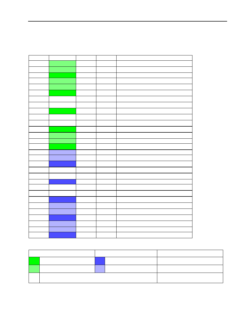
Tables
Page
Table 1. Absolute Maximum Ratings .......................... 3
Table 2. TB64-Type Transponder, Transmitter
Input/Output Pin Descriptions ....................... 5
Table 3. TB64-Type Transponder, Receiver
Input/Output Pin Descriptions ....................... 8
Table 4. Transponder Pin Map.................................. 10
Table 5. TB64-Type Transponder Truth Table
(Transmitter)................................................ 11
Table 6. TB64-Type Transponder Truth Table
(Receiver) ................................................... 12
Table 7. TB64-Type Transponder Pin-Map
Definitions..................................................13
Table 8. Receiver Electrical I/O Characteristics .....23
Table 9. Transmitter Electrical I/O Characteristics...24
Table 10. OC-192/STM-64 Transmitter Optical
Characteristics...........................................26
Table 11. OC-192/STM-64 Receiver Optical
Characteristics...........................................26
Table 12. Power Supply Characteristics ...................26
Table 13. TB64 Transponder Receiver
Timing Characteristics ...............................27
Table 14. TB64 Transponder Transmitter
Timing Characteristics ...............................28
Table 15. Regulatory and Voluntary Compliance.......32
Table 16. Ordering Information ..................................34
Figures
Page
Figure 1. TB64-Type Transponder
Block Diagram..............................................4
Figure 2. Transmitter Block Diagram...........................5
Figure 3. Receiver Block Diagram ..............................8
Figure 4. TB64-Type Transponder Receiver
Timing Characteristics
27
Figure 5. TB64-Type Transponder Transmitter
Timing Characteristics................................28
Figure 6. TB64-Type Receiver Interface
Board Layout..............................................29
Figure 7. TB64-Type Transmitter Interface
Board Layout..............................................30
Figure 8. Recommended Grounding Scheme...........31
Figure 9. Mechanical Dimensions .............................33
Conventions
All signals referenced in italics are for future use.

Data Sheet
March 2003
TB64-Type 10 Gb/s Lightwave Transponder
with 16-Ch. 622 Mb/s MUX/DeMUX and Selectable FEC Rate
For additional information and latest specifications, see our website: www.triquint.com
3
Description
(continued)
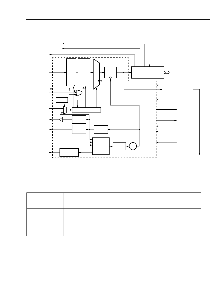
Figure 1 shows a simplified block diagram of the TB64-
type transponder.
In the transmitting direction, the transceiver module
multiplexes sixteen 622.08 Mb/s differential LVDS com-
patible electrical data signals into an optical signal at
9.95328 Gb/s for launching into optical fiber. The opti-
cal transmitter is available with an uncooled, direct-
modulated 1310 nm laser for up to 12 km, short-reach
applications. The TB64-type transponder is thereby
ideally suited for short-reach applications of up to
12 km (SR-1), intraoffice-reach of up to 2 km (I-64.l),
and very short-reach of up to 600 m (VSR). An optional
reference clock cleanup circuit within the TB64 pro-
vides improved jitter performance. The optical output
signal is SONET and ITU compliant for OC-192/STM-
64 applications as shown in Table 10 on page 26.
In the receiving direction, the transceiver module
receives a 9.95328 Gb/s optical signal and converts it
to an electrical signal, extracts a clock signal, and then
demultiplexes the data into sixteen 622 Mb/s differen-
tial LVDS compatible data signals. The receiver oper-
ates over the wavelength range of 1.1
µm to 1.6 µm,
and is fully compliant to SONET/SDH OC-192/STM-64
physical layer specifications as shown in Table 11 on
page 26.
Note that all signals referenced in italics in this docu-
ment are for future use.
Absolute Maximum Ratings
Stresses in excess of the absolute maximum ratings can cause permanent damage to the device. These are abso-
lute stress ratings only. Functional operation of the device is not implied at these or any other conditions in excess
of those given in the operations sections of the data sheet. Exposure to absolute maximum ratings for extended
periods can adversely affect reliability.
1. Note that this device meets NEBS GR63 requirements of operation at 70 ∞C for 14 days (Max) per year, or 96 hours of continuous operation.
2. Human-body target model is 500 V.
Table 1. Absolute Maximum Ratings
Parameter
Symbol
Min
Max
Unit
Operating Case Temperature Range
T
C
0
65
1
∞C
Storage Case Temperature Range
T
S
≠40
85
∞C
≠5.2 V Supply Voltage
V
EE
0.5
≠5.5
V
3.3 V Supply Voltage
V
DD
≠0.5
3.6
V
5.0 V Supply Voltage
V
CC
≠0.5
5.5
V
Voltage on Any LVDS Pin
--
0
V
CC
--
High-speed LVDS Output Source Current
--
--
50
mA
Static Discharge Voltage
2
ESD
--
500
V
Relative Humidity (noncondensing)
RH
--
85
%
Receiver Maximum Input Power PIN Diode
P
IN
--
8.0
dBm
Minimum Fiber Bend Radius
--
1.25 (31.8)
--
in. (mm)

4
For additional information and latest specifications, see our website: www.triquint.com
TB64-Type 10 Gb/s Lightwave Transponder
Data Sheet
with 16-Ch. 622 Mb/s MUX/DeMUX and Selectable FEC Rate
March 2003
Block Diagram
Figure 1. TB64-Type Transponder Block Diagram
LsENABLE
LsBIASMON
LsBIASALM
ANALOG
F18
F24
D18
LsPOWMON
LVTTL
ANALOG
TxDIN[15:0]P/N
LVDS
622
DATA
RETIME
TxFIFOERR
TxFIFORES
K30
K27
LVTTL
LVTTL
DECODE
TIMING GENERATION
TxPICLKP/N
G28,
LVDS
TxMCLKP/N
(155 MHz CLK)
TxPCLKP/N
TxREFCLKP/N
TxREFSEL
TxLOCKERR
DIVIDE
BY 4
MANUAL
PHASE
ADJUST
ACQUISITION
INDICATOR
DIVIDE
BY 16
PHASE AND
FREQUENCY
DETECTOR
CHARGE
PUMP
VCO
LVDS
LVDS
C28,
E28, E29
A28, A29
F30
LVTTL
B30
LVTTL
OC-192/STM-64 OPTICAL
TRANSMITTER
LVTTL
H27 TxLLOOPENB
Tx10GbLOOPBACKDP/N
(ELECTRICAL)
LVTTL
K24
TxRESET
OPEN DRAIN, LVTTL
H15
ALM INT
LVTTL
K21/J21
TxRATESEL[1:0]
B18, B21
TxSKEWSEL[1:0]
B27
TxPICLKSEL
FROM TRANSMITTER
OC-192/STM-OPTICAL
RECEIVER
SAMPLER
CIRCUIT
DIVIDE
BY 16
LVTTL
H6
RxLOOPENB
RxPOWMON
RxPOWALM
RxSIGMON
RxSIGALM
RxRATESEL[1:0]
F3
F6
F9
F12
K3/J3
ANALOG
LVTTL
ANALOG
LVTTL
LVTTL
DATA PHASE/
FREQUENCY
DETECTION
DIVIDE
BY 1 OR
DIVIDE
BY 4
0
1
RxMUTE
DOUT
B6
RxDOUT[15:0]P/N
RxPOCLKP/N
E13/E14
RxMUTEPOCLK
RxMCLKSEL
RxMCLKP/N
RxMUTEMCLK
RxREFSEL
RxREFCLKP/N
LVTTL
1
0
0
1
CHARGE
PUMP
VCO
G29
C29
LVDS OR LVPECL
LVTTL
LVTTL
LVTTL
1
0
LVDS
LVDS
K9 LVTTL
B12 LVTTL
C13/C14 LVDS RECOVERED
CLOCK OUTPUT
LVDS OR LVPECL
LVTTL
K12
A13/A14
F15
RxRESET
RxLCKREF
RxTRACE
I2CCLOCK
I2CDATA
LVTTL
K6
LVTTL
ANALOG
B9
J1
K15
K18
INP
U
T
REGI
STER
DATA
BUFFER
1
6:
1
M
U
LTI
P
LE
X
E
R
OUTPUT REGI
STER
1:
16
DEMU
LT
I
P
LE
XER
RxLOCKERR
B15
LVTTL
Mb/s
F21 LVTTL
LVTTL
D24/D27
TxPHSADJ[1:0]
1-1296 (F).a
For additional information and latest specifications, see our website: www.triquint.com
5
Data Sheet
TB64-Type 10 Gb/s Lightwave Transponder
March 2003
with 16-Ch. 622 Mb/s MUX/DeMUX and Selectable FEC Rate
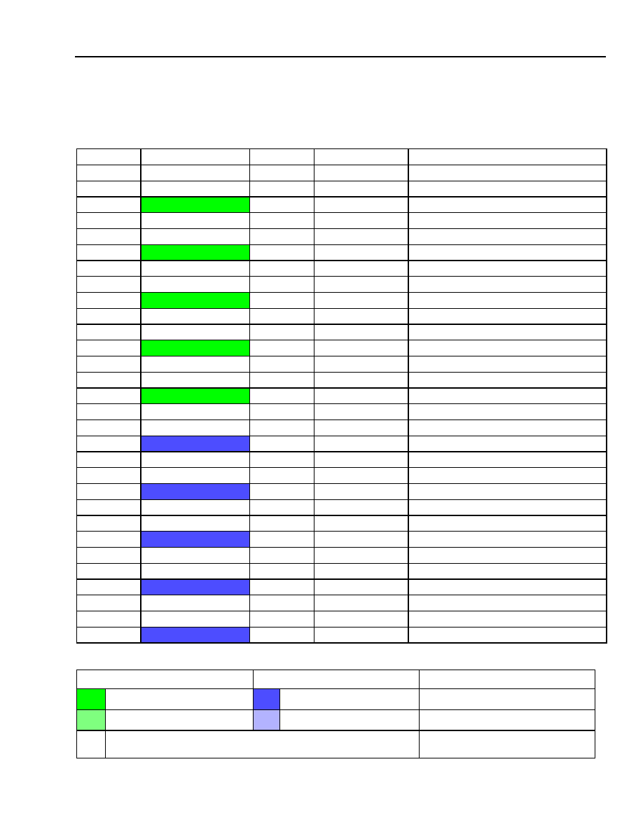
Pin Information
Figure 2. Transmitter Block Diagram
Transmitter Input/Output Pin Descriptions
Table 2. TB64-Type Transponder, Transmitter Input/Output Pin Descriptions
Pin Name
Pin Description
L
S
ENABLE
Laser Enable Input. A logic low on this input pin enables the transmitter's laser. A
logic high disables the laser so there is no optical output.
L
S
BIASMON
Laser Bias Monitor Voltage (Analog). Provides a measure of the laser's dc bias
current as well as an indication of the health of the laser in the transmitter. This out-
put power changes at the rate of 20 mV/mA of bias current to the laser. All of the
monitoring voltage is defined with respect to GND.
LsBIASALM
Laser Bias Alarm. This alarm will go active-low when the bias current to the laser
increases by 50% from its beginning-of-life (BOL) value.
LsENABLE
LsBIASMON
LsBIASALM
LsPOWMON
TxDIN[15:0]P/N
DATA
RETIME
TxFIFOERR
TxFIFORES
DECODE
TIMING GENERATION
TxPICLKP/N
TxMCLKP/N
(155 MHz CLK)
TxPCLKP/N
TxREFCLKP/N
TxREFSEL
TxLOCKERR
DIVIDE
BY 4
MANUAL
PHASE
ADJUST
ACQUISITION
INDICATOR
DIVIDE
BY 16
PHASE AND
FREQUENCY
DETECTOR
CHARGE
PUMP
VCO
OC-192/STM-64 OPTICAL
TRANSMITTER
TxLLOOPENB
Tx10GbLOOPBACKDP/N
(ELECTRICAL)
TxRESET
ALMINT
TxRATESEL[1:0]
TxSKEWSEL[1:0]
TxPICLKSEL
INP
U
T
REGI
STER
DATA
BUFFER
16:
1 MULTIP
LEX
E
R
TO RECEIVER
622
Mb/s
TxPHSADJ[1:0]
1-1297F.a

6
For additional information and latest specifications, see our website: www.triquint.com
Data Sheet
March 2003
TB64-Type 10 Gb/s Lightwave Transponder
with 16-Ch. 622 Mb/s MUX/DeMUX and Selectable FEC Rate
L
S
POWMON
Normalized Laser Power Monitor Voltage (Analog). Provides an indication of the
optical output power level from the transmitter laser. LsPOWMON amplifier gain is
normalized to 500 mV for the nominal transmitter optical output power. If the optical
power decreases by 3 dB from the beginning of life (BOL), this output will drop to
approximately 250 mV. Back-facet monitor transfer function varies from module to
module, and as long as the automatic power control loop is working, the laser output
power remains constant. LsPOWMON is not an alarm signal but rather a perfor-
mance-monitoring feature. The user can measure the transmitter aging by summa-
rizing the laser bias variation, temperature changes, and output power at the same
time.
T
X
D
IN
[15:0]P/N
16-bit Differential LVDS Parallel Data Input. T
X
D
IN
15P/N is the most significant bit
of the input word and is the first bit serialized. T
X
D
IN
0P/N is the least significant bit of
the input word and is the last bit serialized. T
X
D
IN
[15:0]P/N is sampled on the rising
edge of TxPICLK (when TxPICLKSEL = 0) or on the rising and falling edge of
TxPICLK (when TxPICLKSEL = 1). Note that this data will scale when operating at
the FEC rate. Internally biased and terminated.
TxFIFOERR
Transmit FIFO Data Storage Overflow. Indicates active-low when an overflow has
occurred in the parallel data storage element. Operationally, when TxFIFOERR
occurs, the transponder automatically recenters the pointers in the parallel data stor-
age element for fastest FIFO overrun recovery.
TxREFCLKP/N
622.08 MHz or 155.52 MHz Input Reference Clock. This input is used as the refer-
ence for the internal clock frequency synthesizer inside the MUX that generates the
9.9538 GHz bit-rate clock used to shift data out of the parallel-to-serial converter.
Note that this clock frequency must scale when operating at the FEC rate. Internally
ac coupled and biased.
TxREFSEL
Transmitter Reference Select. Used for selection of the TxREFCLK frequency.
Logic 0 is for 155 MHz, logic 1 or no connection for 622 MHz.
T
X
PCLKP/N
Transmitter Parallel Clock. A 622.08 MHz differential output reference parallel
clock. It is normally used to coordinate transfers between customer board logic and
the MUX device. Note that this clock will scale when operating at the FEC rate.
TxPHASADJ[1:0]
Transmitter Phase Adjust. Adjusts phase of TxPCLKP/N clock in 90∞ steps.
TxLOCKERR
Lock Detect/Phase Error (Active-Low). It goes low when MUX PLL has not locked
to the TxREFCLK.
TxMCLKP/N
Transmitter 155 MHz Clock Output from the Clock Synthesizer of the MUX. This
output can be connected to the reference clock input of the deMUX chip, thereby
eliminating the need for a separate RxREFCLK VCO on the customer board. Note
that this clock will scale when operating at the FEC rate.
TxPICLKP/N
Differential LVDS Compatible Parallel Input Clock. A 622.08 MHz nominally 50%
duty cycle input clock, to which TxDin[15:0]P/N is aligned. TxPICLK is used to trans-
fer the data on the 16 TxD
IN
inputs into the holding register in the parallel-to-serial
converter. Note that this clock will scale when operating at the FEC rate. Internally
biased and terminated.
TxPICLKSEL
TxPICLK Clock Select. Used to select between the 622.08 MHz or 311.04 MHz
dual-edge clock options of the TxPICLKP/N. Logic 0 is for 622.08 MHz, and logic 1 is
for 311.04 MHz.
Table 2. TB64-Type Transponder, Transmitter Input/Output Pin Descriptions (continued)
Pin Name
Pin Description
Pin Information
(continued)
Transmitter Input/Output Pin Descriptions
(continued)

For additional information and latest specifications, see our website: www.triquint.com
7
Data Sheet
March 2003
TB64-Type 10 Gb/s Lightwave Transponder
with 16-Ch. 622 Mb/s MUX/DeMUX and Selectable FEC Rate
TxRESET
MUX Master Reset. Reset input for the device. Reset must be held active-low for a
minimum of 6.4 ns. During a reset, the true data outputs are in the logic low state.
For normal power sequencing on power-up, no reset is required.
ALMINT
Alarm Interrupt (Active-Low). Combined logic level (OR) output of RxPOWALM,
RxSIGALM, RxLOCKERR, LsBIASALM, and TxLOCKERR. The signal is an open
drain-type LVTTL output.
TxRATESEL[1:0]
Transmitter Rate Select, FEC Rate Select (Active-Low). Selects the normal
OC-192/STM-64 rate of 9.9532 GHz, 10 GbE Ethernet rate of 10.3 Gb/s or the FEC
rate of 10.6642 GHz:
x, 0 = FEC rate of 10.6642 Gb/s/10.709 Gb/s, selected with TxREFCLK
x, 1 = OC-192/STM-64 rate of 9.9532 Gb/s or 10GbE rate of 10.312 Gb/s, selected
with TxREFCLK
where x is either 0 or 1.
Note that all input and output clock and data rates are scaled appropriately when
operating at the FEC rate.
TxFIFORES
TxLOOPENB
TxSKEWSEL[1:0]
Pins reserved in MSA. Functions not implemented.
Table 2. TB64-Type Transponder, Transmitter Input/Output Pin Descriptions (continued)
Pin Name
Pin Description
Pin Information
(continued)
Transmitter Input/Output Pin Descriptions
(continued)

8
For additional information and latest specifications, see our website: www.triquint.com
TB64-Type 10 Gb/s Lightwave Transponder
Data Sheet
with 16-Ch. 622 Mb/s MUX/DeMUX and Selectable FEC Rate
March 2003
Pin Information
(continued)
Figure 3. Receiver Block Diagram
Receiver Input/Ou
tpu
t Pin Descriptions
Table 3. TB64-Type Transponder, Receiver Input/Output Pin Descriptions
Pin Name
Pin Description
R
X
LOCKERR
Clock Recovery Error Indicator (Active-Low). Indicates when the internal clock recov-
ery has not locked onto the incoming data stream. RxLOCKERR is an asynchronous out-
put.
R
X
REFCLKP/N
Differential ac-Coupled Reference Clock Input at 155.52 MHz or 622 MHz. The PLL
inside the deMUX will lock onto this reference in absence of optical serial input data. Note
that this clock frequency must scale to the appropriate reference rate when not operating
at the standard OC-192 SONET/SDH rate. Internally ac coupled and biased.
RxREFSEL
R
X
REFCLK Frequency Selector. Logic 0 for 155 MHz (divide by 64) and logic 1 or no
connections for 622 MHz (divide by 16).
R
X
D
OUT
[15:0]P/N
16-bit Differential LVDS Parallel Output Data Bus. D
OUT
[15:0] is the 622 Mb/s 16-bit
output word. D
OUT
15P/N is the most significant bit of the received word and is the first bit
received. D
OUT
0P/N is the least significant bit of the received word and is the last bit
received. Note that this clock frequency must scale to the appropriate reference rate when
not operating at the standard OC-192 SONET/SDH rate. Internally ac coupled and biased.
R
X
POCLKP/N
Recovered Differential LVDS Parallel Output Clock of 622 MHz (Nominally 50% Duty
Cycle). This clock is recovered from the incoming optical signal and is aligned to the
D
OUT
[15:0] output data. When RxPOCLKP/N is not locked to the incoming data signal,
RxLOCKERR will be forced low. Pins are active but forced to differential logic low when
RxMUTE D
OUT
= 0. Note that this clock frequency must scale to the appropriate reference
rate when not operating at the standard OC-192 SONET/SDH rate. Internally ac coupled
and biased.
RxMUTEPOCLK
Disables the output clock of 622 MHz.
RxPOWMON
Input Power Monitor Voltage (Analog). Provides a relative measure of the average input
optical (ac + dc) power to the receiver. This signal is referenced to ground. Output voltage
to input optical transfer function is 1.0 V/mW.
FROM TRANSMITTER
RxLOOPBACKDATA
(ELECTRICAL)
OC-192/STM-OPTICAL
RECEIVER
SAMPLER
CIRCUIT
DIVIDE
BY 16
RxDLOOPENB
RxPOWMON
RxPOWALM
RxSIGMON
RxSIGALM
RxRATESEL[1:0]
DATA PHASE/
FREQUENCY
DETECTION
DIVIDE
BY 1 OR
DIVIDE
BY 4
0
1
RxMUTE
DOUT
RxDOUT[15:0]P/N
RxPOCLKP/N
RxMUTEPOCLK
RxMCLKSEL
RxMCLKP/N
RxMUTEMCLK
RxREFSEL
RxREFCLKP/N
1
0
0
1
CHARGE
PUMP
VCO
1
0
RECOVERED
CLOCK OUTPUT
RxRESET
RxLCKREF
RxTRACE
I2CCLOCK
I2CDATA
OUT
P
UT
1:
16 DEMULTIP
LEX
E
R
RxLOCKERR
REGISTE
R
1-1282 (F).a

For additional information and latest specifications, see our website: www.triquint.com
9
Data Sheet
March 2003
TB64-Type 10 Gb/s Lightwave Transponder
with 16-Ch. 622 Mb/s MUX/DeMUX and Selectable FEC Rate
RxPOWALM
Receive Power Alarm. This alarm goes active low when the received average optical
power drops below a threshold level. When the input power increases above the threshold
level by 1dB (i.e. hysteresis is 1dB), the alarm is cleared.
RxRATESEL[1:0]
Receiver Rate Select (Active-Low). Selects the normal OC-192/STM-64 rate, 10 GbE
rate, or FEC rate:
x, 0 = FEC rate of 10.6642/10.709 Gb/s, selected with TxREFCLK
x, 1 = OC-192/STM-64 rate of 9.9532 Gb/s or 10GbE rate of 10.312 Gb/s, selected with
TxREFCLK
where x is either 0 or 1.
Note that all input and output clock and data rates are scaled appropriately when operat-
ing at the FEC rate.
R
X
MCLKP/N
Receiver 155 MHz or 622 MHz Output Clock.
RxMUTEMCLK
When RxMUTEMCLK is 0, it mutes RxMCLK. Normal operation, when RxMUTEMCLK is
1.
RxMCLKSEL
When 0, RxMCLKSEL selects the RxMCLK frequency of 155 MHz. When 1, RxMCLKSEL
selects the RxMCLK frequency of 622 MHz.
RxRESET
Active-low. Resets all synchronous logic. During a reset, the data outputs are in the logic
low state. Reset must be held active-low for a minimum of 6.4 ns while the internal oscilla-
tor is active:
0 = reset
1 or no connection = normal operation
RxDLOOPENB
Diagnostic Loopback Enable (Active-Low). Enables diagnostic loopback (10 Gb/s MUX
to 10 Gb/s deMUX).
RxMUTED
OUT
Receiver Mute D
OUT
(Active-Low). When RxMUTED
OUT
is active, it forces all deMUX
output data RxDout[15:0]P/N to a logic low level. When RxMUTED
OUT
is inactive, data to
the deMUX will be processed normally.
0 = deMUX output muted.
1 or no connection = normal operation.
I
2
CCLOCK
I
2
CDATA
RxSIGMON
RxSIGALM
RxLCKREF
RxTRACE
Pins reserved in MSA. Functions not implemented.
Table 3. TB64-Type Transponder, Receiver Input/Output Pin Descriptions
Pin Name
Pin Description
Pin Information
(continued)
Receiver Input/Output Pin Descriptions
(continued)

10
For additional information and latest specifications, see our website: www.triquint.com
TB64-Type 10 Gb/s Lightwave Transponder
Data Sheet
with 16-Ch. 622 Mb/s MUX/DeMUX and Selectable FEC Rate
March 2003
Pin Information
(continued)
Transponder Pin Map
* This feature is only available on lasers using thermoelectric coolers. For uncooled transponders, the associated pin is considered NUC.
Table 4. Transponder Pin Map
Receiver Section
K
J
H
G
F
E
D
C
B
A
1 5.0 V Analog RxTRACE
Frame GND RxD
OUT
12P 1.8 V Digital RxD
OUT
8P Digital
GND RxD
OUT
4P
Digital
GND
RxD
OUT
0P
2 5.0 V Analog
FFU
Frame GND RxD
OUT
12N 1.8 V Digital RxD
OUT
8N Digital
GND RxD
OUT
4N
Digital
GND
RxD
OUT
0N
3 RxRATESEL0
RxRATESEL1
FFU
Digital GND RxPOWMON Digital
GND
FFU
Digital
GND
FFU
Digital
GND
4 3.3 V Analog
NUC
Frame GND RxDOUT13P 3.3 V Digital RxD
OUT
9P Digital
GND RxD
OUT
5P
Digital
GND
RxD
OUT
1P
5 3.3 V Analog
NUC
Frame GND RxDOUT13N 3.3 V Digital RxD
OUT
9N Digital
GND RxD
OUT
5N
Digital
GND
RxD
OUT
1N
6
RxRESET
NUC
RxDLOOPENB
Digital GND RxPOWALM Digital
GND
FFU
Digital
GND RxMUTED
OUT
Digital
GND
7
FFU
FFU
Analog GND
RxD
OUT
14P 3.3 V Digital RxD
OUT
10P Digital
GND RxD
OUT
6P
Digital
GND
RxD
OUT
2P
8
FFU
FFU
Analog GND
RxD
OUT
14N 3.3 V Digital RxD
OUT
10N Digital
GND RxD
OUT
6N
Digital
GND
RxD
OUT
2N
9
RxMUTEPOCLK
NUC
FFU
Digital GND RxSIGMON Digital
GND
FFU
Digital
GND RxLCKREF
Digital
GND
10 ≠5.2 V Analog
FFU
Analog GND
RxD
OUT
15P ≠5.2 V Digital RxD
OUT
11P Digital
GND RxD
OUT
7P
Digital
GND
RxD
OUT
3P
11 ≠5.2 V Analog
FFU
Analog GND
RxD
OUT
15N ≠5.2 V Digital RxD
OUT
11N Digital
GND RxD
OUT
7N
Digital
GND
RXD
OUT
3N
12
RxMUTEMCLK
NUC
FFU
Digital GND
RxSIGALM Digital
GND
FFU
Digital
GND RxMCLKSEL Digital
GND
13 ≠5.2 V Analog
FFU
Analog GND
FFU
≠5.2 V Digital RxPOCLKP Digital
GND RxMCLKP
Digital
GND RxREFCLKP
14 ≠5.2 V Analog RxALMINT Analog GND
FFU
≠5.2 V Digital RxPOCLKN Digital
GND RxMCLKN
Digital
GND RxREFCLKN
15 I
2
CCLOCK
NUC
ALMINT
Digital GND RxREFSEL Digital
GND
FFU
Digital
GND RxLOCKERR Digital
GND
Transmitter Section
K
J
H
G
F
E
D
C
B
A
16 5.0 V Analog
TxALMINT
Analog GND
TxD
IN
12P
1.8 V Digital
TxD
IN
8P
Digital
GND
TxD
IN
4P
Digital
GND
TxD
IN
0P
17 5.0 V Analog
FFU
Analog GND
TxD
IN
12N
1.8 V Digital
TxD
IN
8N
Digital
GND
TxD
IN
4N
Digital
GND
TxD
IN
0N
18
I
2
CDATA
NUC
LsTUNE0*
Digital GND LsBIASMON Digital
GND LsPOWMON Digital
GND TxSKEWSEL0 Digital
GND
19 3.3 V Analog
FFU
Analog GND
TxD
IN
13P
3.3 V Digital
TxD
IN
9P
Digital
GND
TxD
IN
5P
Digital
GND
TxD
IN
1P
20 3.3 V Analog
FFU
Analog GND
TxD
IN
13N
3.3 V Digital
TxD
IN
9N
Digital
GND
TxD
IN
5N
Digital
GND
TxD
IN
1N
21 TxRATESEL0
TxRATESEL1
LsTUNE1*
Digital GND
LsENABLE Digital
GND
LsTEMPMON*
Digital
GND TxSKEWSEL1 Digital
GND
22 3.3 V Analog
FFU
Analog GND
TxD
IN
14P
3.3 V Digital TxD
IN
10P Digital
GND
TxD
IN
6P
Digital
GND
TxD
IN
2P
23 3.3 V Analog
FFU
Analog GND
TxD
IN
14N
3.3 V Digital TxD
IN
10N Digital
GND
TxD
IN
6N
Digital
GND
TxD
IN
2N
24
TxRESET
NUC
LsTUNE2*
Digital GND LsBIASALM Digital
GND TxPHSADJ0 Digital
GND L
S
TWEAK*
Digital
GND
25 ≠5.2 V Analog
NUC
Frame GND
TxD
IN
15P ≠5.2 V Digital TxD
IN
11P
Digital
GND
TxD
IN
7P
Digital
GND
TxD
IN
3P
26 ≠5.2 V Analog
NUC
Frame GND
TxD
IN
15N ≠5.2 V Digital TxD
IN
11N Digital
GND
TxD
IN
7N
Digital
GND
TxD
IN
3N
27 TxFIFORES
NUC
TxLLOOPENB
Digital GND
L
S
TEMPALM*
Digital
GND TxPHSADJ1 Digital
GND TxPICLKSEL Digital
GND
28 ≠5.2 V Analog
FFU
Frame GND
TxPICLKP ≠5.2 V Digital TxPCLKP Digital
GND TxMCLKP
Digital
GND TxREFCLKP
29 ≠5.2 V Analog TxTRACE
Frame GND
TxPICLKN ≠5.2 V Digital TxPCLKN Digital
GND TxMCLKN
Digital
GND TxREFCLKN
30 TxFIFOERR
NUC
TxLINETIMSEL
D
IGital
GND
TxREFSEL Digital
GND
FFU
Digital
GND TxLOCKERR Digital
GND
Receiver Section
Transmitter Section
Other
Rx power and GND supplies
Tx power and GND supplies
NUC: no user connection
Rx dc signals
Tx dc signals
FFU: reserved for future use
622 Mb/s differential signals (transmitter and receiver sections)
Italics: future feature (not
immediately available)

For additional information and latest specifications, see our website: www.triquint.com
11
Data Sheet
TB64-Type 10 Gb/s Lightwave Transponder
March 2003
with 16-Ch. 622 Mb/s MUX/DeMUX and Selectable FEC Rate
Pin Information
(continued)
Truth Tables
1. TxPICLK frequency of 622 MHz is the MSA standard. The TxPICLK function should be tied to ground when not used.
Table 5. TB64-Type Transponder Pin-Map Truth Table (Transmitter)
Pin Name and Pin
Configuration
Description
LsENABLE
0
1
Normal Operation.
Laser Disabled.
LsBIASALM
0
1
Laser Bias Alarm Active.
Normal Operation.
TxREFSEL
0
1
Selects a TxREFCLK Frequency of 155 MHz.
Selects a TxREFCLK Frequency of 622 MHz.
TxPICLKSEL
1
0
1
Selects the TxPICLK Frequency of 622 MHz.
Selects the TxPICLK Frequency of 311 MHz.
TxLOCKERR
0
1
Indicates Loss of PLL Lock.
Normal Operation.
TxRESET
0
1
Asynchronous MUX System Reset.
Normal Operation.
TxFIFOERR
0
1
Indicates a MUX FIFO Error.
Normal Operation.
ALMINT
0
1
Indicates an Alarm.
Normal Operation.
TxRATESEL1
0 or 1
0 or 1
TxRATESEL0
0
1
FEC rate of 10.6642 Gb/s or 10.7092 Gb/s.
OC-192/STM-64 rate of 9.9532 GHz or 10GbE rate of 10.3125 Gb/s.
TxPHSADJ1
0
0
1
1
TxPHSADJ0
0
1
0
1
Adjusts the Phase of the TxPLCK by 0∞.
Adjusts the Phase of the TxPLCK by 90∞.
Adjusts the Phase of the TxPLCK by 180∞.
Adjusts the Phase of the TxPLCK by 270∞.

12
For additional information and latest specifications, see our website: www.triquint.com
TB64-Type 10 Gb/s Lightwave Transponder
Data Sheet
with 16-Ch. 622 Mb/s MUX/DeMUX and Selectable FEC Rate
March 2003
Pin Information
(continued)
Truth Tables
(continued)
Table 6. TB64-Type Transponder Pin-Map Truth Table (Receiver)
Pin Name and Pin Configuration
Description
RxRESET
0
1
Asynchronous DeMUX System Reset.
Normal Operation.
RxMUTEPOCLK
0
1
Mutes the RxPOCLK.
Normal Operations.
RxMUTEMCLK
0
1
Mutes the RxMCLK.
Normal Operations.
RxDLOOPENB
0
1
Enables Diagnostic Loopback (10 Gb/s MUX to 10 Gb/s DeMUX).
Normal Operation.
RxMUTEDOUT
0
1
Mutes the RxDOUT[15:0].
Normal Operation.
RxLCKREF
0
1
RxPOCLK Locks to RxREFCLK.
Normal Operation.
RxMCLKSEL
0
1
Selects the RxMCLK Frequency of 155 MHz.
Selects the RxMCLK Frequency of 622 MHz.
RxLOCKERR
0
1
Indicates Loss of PLL Lock.
Normal Operation.
RxPOWALM
0
1
Indicates Alarm Active.
Normal Operation.
RxSIGALM
0
1
Indicates Alarm Active.
Normal Operation.
RxREFSEL
0
1
Selects an RxREFCLK Frequency of 155 MHz.
Selects an RxREFCLK Frequency of 622 MHz.
RxRATESEL1
0 or 1
0 or 1
RxRATESEL0
0
1
FEC rate of 10.6642 Gb/s or 10.7092 Gb/s.
OC-192/STM-64 rate of 9.9532 GHz or 10GbE rate of 10.3125 Gb/s.
For additional information and latest specifications, see our website: www.triquint.com
13
Data Sheet
TB64-Type 10 Gb/s Lightwave Transponder
March 2003
with 16-Ch. 622 Mb/s MUX/DeMUX and Selectable FEC Rate
Pin Information
(continued)
Pin-Map Definitions
Table 7. TB64-Type Transponder Pin-Map Definitions
Pin #
Pin Name
I/O
Logic
Description
A1
R
X
D
OUT
0P
O
LVDS
Receiver 622 Mb/s Data Output.
A2
R
X
D
OUT
0N
O
LVDS
Receiver 622 Mb/s Data Output.
A3
Digital GND
I
Supply
Receiver Digital Ground.
A4
R
X
D
OUT
1P
O
LVDS
Receiver 622 Mb/s Data Output.
A5
R
X
D
OUT
1N
O
LVDS
Receiver 622 Mb/s Data Output.
A6
Digital GND
I
Supply
Receiver Digital Ground.
A7
R
X
D
OUT
2P
O
LVDS
Receiver 622 Mb/s Data Output.
A8
R
X
D
OUT
2N
O
LVDS
Receiver 622 Mb/s Data Output.
A9
Digital GND
I
Supply
Receiver Digital Ground.
A10
R
X
D
OUT
3P
O
LVDS
Receiver 622 Mb/s Data Output.
A11
R
X
D
OUT
3N
O
LVDS
Receiver 622 Mb/s Data Output.
A12
Digital GND
I
Supply
Receiver Digital Ground.
A13
R
X
REFCLKP
I
LVDS or LVPECL Receiver Reference Clock.
A14
R
X
REFCLKN
I
LVDS or LVPECL Receiver Reference Clock.
A15
Digital GND
I
Supply
Receiver Digital Ground.
A16
T
X
D
IN
0P
I
LVDS
Transmitter 622 Mb/s Data Input.
A17
T
X
D
IN
0N
I
LVDS
Transmitter 622 Mb/s Data Input.
A18
Digital GND
I
Supply
Transmitter Digital Ground.
A19
T
X
D
IN
1P
I
LVDS
Transmitter 622 Mb/s Data Input.
A20
T
X
D
IN
1N
I
LVDS
Transmitter 622 Mb/s Data Input.
A21
Digital GND
I
Supply
Transmitter Digital Ground.
A22
T
X
D
IN
2P
I
LVDS
Transmitter 622 Mb/s Data Input.
A23
T
X
D
IN
2N
I
LVDS
Transmitter 622 Mb/s Data Input.
A24
Digital GND
I
Supply
Transmitter Digital Ground.
A25
T
X
D
IN
3P
I
LVDS
Transmitter 622 Mb/s Data Input.
A26
T
X
D
IN
3N
I
LVDS
Transmitter 622 Mb/s Data Input.
A27
Digital GND
I
Supply
Transmitter Digital Ground.
A28
TxREFCLKP
I
LVDS or LVPECL Transmitter Reference Clock.
A29
TxREFCLKN
I
LVDS or LVPECL Transmitter Reference Clock.
A30
Digital GND
I
Supply
Transmitter Digital Ground.
Receiver Section
Transmitter Section
Other
Rx power and GND supplies
Tx power and GND supplies
NUC: no user connection
Rx dc signals
Tx dc signals
FFU: reserved for future use
622 Mb/s differential signals (transmitter and receiver sections)
Italics: future feature (not
immediately available)

14
For additional information and latest specifications, see our website: www.triquint.com
TB64-Type 10 Gb/s Lightwave Transponder
Data Sheet
with 16-Ch. 622 Mb/s MUX/DeMUX and Selectable FEC Rate
March 2003
Pin Information
(continued)
Pin-Map Definitions
(continued)
Table 7. TB64-Type Transponder Pin-Map Definitions (continued)
Pin #
Pin Name
I/O
Logic
Description
B1
Digital GND
I
Supply
Receiver Digital Ground.
B2
Digital GND
I
Supply
Receiver Digital Ground.
B3
FFU
--
--
Reserved for Future Use.
B4
Digital GND
I
Supply
Receiver Digital Ground.
B5
Digital GND
I
Supply
Receiver Digital Ground.
B6
R
X
MUTED
OUT
I
LVTTL
Mutes the Data Outputs of the DeMUX.
B7
Digital GND
I
Supply
Receiver Digital Ground.
B8
Digital GND
I
Supply
Receiver Digital Ground.
B9
R
X
LCKREF
I
LVTTL
Locks R
X
POCLK to RxREFCLK.
B10
Digital GND
I
Supply
Receiver Digital Ground.
B11
Digital GND
I
Supply
Receiver Digital Ground.
B12
R
X
MCLKSEL
I
LVTTL
Selects Speed of Output R
X
MCLK.
B13
Digital GND
I
Supply
Receiver Digital Ground.
B14
Digital GND
I
Supply
Receiver Digital Ground.
B15
R
X
LOCKERR
O
LVTTL Loss of Lock of RxPOCLK (active-low).
B16
Digital GND
I
Supply
Transmitter Digital Ground.
B17
Digital GND
I
Supply
Transmitter Digital Ground.
B18
T
X
SKEWSEL0
I
LVTTL
Adjusts Skew of T
X
PICLK (LSB).
B19
Digital GND
I
Supply
Transmitter Digital Ground.
B20
Digital GND
I
Supply
Transmitter Digital Ground.
B21
T
X
SKEWSEL1
I
LVTTL
Adjusts Skew of T
X
PICLK (MSB).
B22
Digital GND
I
Supply
Transmitter Digital Ground.
B23
Digital GND
I
Supply
Transmitter Digital Ground.
B24
L
S
TWEAK
I
Analog
Laser Fine Tuning of DWDM Wavelength.
B25
Digital GND
I
Supply
Transmitter Digital Ground.
B26
Digital GND
I
Supply
Transmitter Digital Ground.
B27
T
X
PICLKSEL
I
LVTTL
Selects Speed of Input T
X
PICLK.
B28
Digital GND
I
Supply
Transmitter Digital Ground.
B29
Digital GND
I
Supply
Transmitter Digital Ground.
B30
TxLOCKERR
O
LVTTL
Indicates Loss of T
X
PLL Lock.
Receiver Section
Transmitter Section
Other
Rx power and GND supplies
Tx power and GND supplies
NUC: no user connection
Rx dc signals
Tx dc signals
FFU: reserved for future use
622 Mb/s differential signals (transmitter and receiver sections)
Italics: future feature (not
immediately available)
For additional information and latest specifications, see our website: www.triquint.com
15
Data Sheet
TB64-Type 10 Gb/s Lightwave Transponder
March 2003
with 16-Ch. 622 Mb/s MUX/DeMUX and Selectable FEC Rate
Pin Information
(continued)
Pin-Map Definitions
(continued)
Table 7. TB64-Type Transponder Pin-Map Definitions (continued)
Pin #
Pin Name
I/O
Logic
Description
C1
R
X
D
OUT
4P
O
LVDS
Receiver 622 Mb/s Data Output.
C2
R
X
D
OUT
4N
O
LVDS
Receiver 622 Mb/s Data Output.
C3
Digital GND
I
Supply
Receiver Digital Ground.
C4
R
X
D
OUT
5P
O
LVDS
Receiver 622 Mb/s Data Output.
C5
R
X
D
OUT
5N
O
LVDS
Receiver 622 Mb/s Data Output.
C6
Digital GND
I
Supply
Receiver Digital Ground.
C7
R
X
D
OUT
6P
O
LVDS
Receiver 622 Mb/s Data Output.
C8
R
X
D
OUT
6N
O
LVDS
Receiver 622 Mb/s Data Output.
C9
Digital GND
I
Supply
Receiver Digital Ground.
C10
R
X
D
OUT
7P
O
LVDS
Receiver 622 Mb/s Data Output.
C11
R
X
D
OUT
7N
O
LVDS
Receiver 622 Mb/s Data Output.
C12
Digital GND
I
Supply
Receiver Digital Ground.
C13
R
X
MCLKP
O
LVDS
VCO-Derived Output Rx Clock.
C14
R
X
MCLKN
O
LVDS
VCO-Derived Output Rx Clock.
C15
Digital GND
I
Supply
Receiver Digital Ground.
C16
T
X
D
IN
4P
I
LVDS
Transmitter 622 Mb/s Data Input.
C17
TXD
IN
4N
I
LVDS
Transmitter 622 Mb/s Data Input.
C18
Digital GND
I
Supply
Transmitter Digital Ground.
C19
T
X
D
IN
5P
I
LVDS
Transmitter 622 Mb/s Data Input.
C20
T
X
D
IN
5N
I
LVDS
Transmitter 622 Mb/s Data Input.
C21
Digital GND
I
Supply
Transmitter Digital Ground.
C22
T
X
D
IN
6P
I
LVDS
Transmitter 622 Mb/s Data Input.
C23
T
X
D
IN
6N
I
LVDS
Transmitter 622 Mb/s Data Input.
C24
Digital GND
I
Supply
Transmitter Digital Ground.
C25
T
X
D
IN
7P
I
LVDS
Transmitter 622 Mb/s Data Input.
C26
T
X
D
IN
7N
I
LVDS
Transmitter 622 Mb/s Data Input.
C27
Digital GND
I
Supply
Transmitter Digital Ground.
C28
TxMCLKP
O
LVDS
VCO-Derived Output Tx Clock.
C29
TxMCLKN
O
LVDS
VCO-Derived Output Tx Clock.
C30
Digital GND
I
Supply
Transmitter Digital Ground.
Receiver Section
Transmitter Section
Other
Rx power and GND supplies
Tx power and GND supplies
NUC: no user connection
Rx dc signals
Tx dc signals
FFU: reserved for future use
622 Mb/s differential signals (transmitter and receiver sections)
Italics: future feature (not
immediately available)
16
For additional information and latest specifications, see our website: www.triquint.com
TB64-Type 10 Gb/s Lightwave Transponder
Data Sheet
with 16-Ch. 622 Mb/s MUX/DeMUX and Selectable FEC Rate
March 2003
Pin Information
(continued)
Pin-Map Definitions
(continued)
Table 7. TB64-Type Transponder Pin-Map Definitions (continued)
Pin #
Pin Name
I/O
Logic
Description
D1
Digital GND
I
Supply
Receiver Digital Ground.
D2
Digital GND
I
Supply
Receiver Digital Ground.
D3
FFU
--
--
Reserved for Future Use.
D4
Digital GND
I
Supply
Receiver Digital Ground.
D5
Digital GND
I
Supply
Receiver Digital Ground.
D6
FFU
--
--
Reserved for Future Use.
D7
Digital GND
I
Supply
Receiver Digital Ground.
D8
Digital GND
I
Supply
Receiver Digital Ground.
D9
FFU
--
--
Reserved for Future Use.
D10
Digital GND
I
Supply
Receiver Digital Ground.
D11
Digital GND
I
Supply
Receiver Digital Ground.
D12
FFU
--
--
Reserved for Future Use.
D13
Digital GND
I
Supply
Receiver Digital Ground.
D14
Digital GND
I
Supply
Receiver Digital Ground.
D15
FFU
--
--
Reserved for Future Use.
D16
Digital GND
I
Supply
Transmitter Digital Ground.
D17
Digital GND
I
Supply
Transmitter Digital Ground.
D18
L
S
POWMON
O
Analog
Laser Output Power Monitor.
D19
Digital GND
I
Supply
Transmitter Digital Ground.
D20
Digital GND
I
Supply
Transmitter Digital Ground.
D21
L
S
TEMPMON
O
Analog
Laser Temperature Monitor.
D22
Digital GND
I
Supply
Transmitter Digital Ground.
D23
Digital GND
I
Supply
Transmitter Digital Ground.
D24
TxPHSADJ0
I
LVTTL
Adjusts Phase of TxPCLK (LSB).
D25
Digital GND
I
Supply
Transmitter Digital Ground.
D26
Digital GND
I
Supply
Transmitter Digital Ground.
D27
TxPHSADJ1
I
LVTTL
Adjusts Phase of TxPCLK (MSB).
D28
Digital GND
I
Supply
Transmitter Digital Ground.
D29
Digital GND
I
Supply
Transmitter Digital Ground.
D30
FFU
--
--
Reserved for Future Use.
Receiver Section
Transmitter Section
Other
Rx power and GND supplies
Tx power and GND supplies
NUC: no user connection
Rx dc signals
Tx dc signals
FFU: reserved for future use
622 Mb/s differential signals (transmitter and receiver sections)
Italics: future feature (not
immediately available)
For additional information and latest specifications, see our website: www.triquint.com
17
Data Sheet
TB64-Type 10 Gb/s Lightwave Transponder
March 2003
with 16-Ch. 622 Mb/s MUX/DeMUX and Selectable FEC Rate
Pin Information
(continued)
Pin-Map Definitions
(continued)
Table 7. TB64-Type Transponder Pin-Map Definitions (continued)
Pin #
Pin Name
I/O
Logic
Description
E1
R
X
D
OUT
8P
O
LVDS
Receiver 622 Mb/s Data Output.
E2
R
X
D
OUT
8N
O
LVDS
Receiver 622 Mb/s Data Output.
E3
Digital GND
I
Supply
Receiver Digital Ground.
E4
R
X
D
OUT
9P
O
LVDS
Receiver 622 Mb/s Data Output.
E5
R
X
D
OUT
9N
O
LVDS
Receiver 622 Mb/s Data Output.
E6
Digital GND
I
Supply
Receiver Digital Ground.
E7
R
X
D
OUT
10P
O
LVDS
Receiver 622 Mb/s Data Output.
E8
R
X
D
OUT
10N
O
LVDS
Receiver 622 Mb/s Data Output.
E9
Digital GND
I
Supply
Receiver Digital Ground.
E10
R
X
D
OUT
11P
O
LVDS
Receiver 622 Mb/s Data Output.
E11
R
X
D
OUT
11N
O
LVDS
Receiver 622 Mb/s Data Output.
E12
Digital GND
I
Supply
Receiver Digital Ground.
E13
R
X
POCLKP
O
LVDS
Receiver Parallel Output Clock.
E14
RXPOCLKN
O
LVDS
Receiver Parallel Output Clock.
E15
Digital GND
I
Supply
Receiver Digital Ground.
E16
T
X
D
IN
8P
I
LVDS
Transmitter 622 Mb/s Data Input.
E17
T
X
D
IN
8N
I
LVDS
Transmitter 622 Mb/s Data Input.
E18
Digital GND
I
Supply
Transmitter Digital Ground.
E19
T
X
D
IN
9P
I
LVDS
Transmitter 622 Mb/s Data Input.
E20
T
X
D
IN
9N
I
LVDS
Transmitter 622 Mb/s Data Input.
E21
Digital GND
I
Supply
Transmitter Digital Ground.
E22
T
X
D
IN
10P
I
LVDS
Transmitter 622 Mb/s Data Input.
E23
TXD
IN
10N
I
LVDS
Transmitter 622 Mb/s Data Input.
E24
Digital GND
I
Supply
Transmitter Digital Ground.
E25
T
X
D
IN
11P
I
LVDS
Transmitter 622 Mb/s Data Input.
E26
TXD
IN
11N
I
LVDS
Transmitter 622 Mb/s Data Input.
E27
Digital GND
I
Supply
Transmitter Digital Ground.
E28
T
X
PCLKP
O
LVDS
Transmitter Parallel Output Clock.
E29
T
X
PCLKN
O
LVDS
Transmitter Parallel Output Clock.
E30
Digital GND
I
Supply
Transmitter Digital Ground.
Receiver Section
Transmitter Section
Other
Rx power and GND supplies
Tx power and GND supplies
NUC: no user connection
Rx dc signals
Tx dc signals
FFU: reserved for future use
622 Mb/s differential signals (transmitter and receiver sections)
Italics: future feature (not
immediately available)
18
For additional information and latest specifications, see our website: www.triquint.com
TB64-Type 10 Gb/s Lightwave Transponder
Data Sheet
with 16-Ch. 622 Mb/s MUX/DeMUX and Selectable FEC Rate
March 2003
Pin Information
(continued)
Pin-Map Definitions
(continued)
Table 7. TB64-Type Transponder Pin-Map Definitions (continued)
Pin #
Pin Name
I/O
Logic
Description
F1
1.8 V Digital
I
Supply
Receiver Digital Power.
F2
1.8 V Digital
I
Supply
Receiver Digital Power.
F3
R
X
POWMON
O
Analog
Receiver Power Monitor (ac + dc).
F4
3.3 V Digital
I
Supply
Receiver Digital Power.
F5
3.3 V Digital
I
Supply
Receiver Digital Power.
F6
RxPOWALM
O
LVTTL
Loss of Receiver Average Power Alarm.
F7
3.3 V Digital
I
Supply
Receiver Digital Power.
F8
3.3 V Digital
I
Supply
Receiver Digital Power.
F9
R
X
SIGMON
O
Analog
Receiver Signal Monitor (ac only).
F10
≠5.2 V Digital
I
Supply
Receiver Digital Power.
F11
≠5.2 V Digital
I
Supply
Receiver Digital Power.
F12
R
X
SIGALM
O
LVTTL
Loss of Receiver ac Power Alarm
F13
≠5.2 V Digital
I
Supply
Receiver Digital Power.
F14
≠5.2 V Digital
I
Supply
Receiver Digital Power.
F15
RxREFSEL
I
LVTTL
Selects R
X
REFCLK Frequency.
F16
1.8 V Digital
I
Supply
Transmitter Digital Power.
F17
1.8 V Digital
I
Supply
Transmitter Digital Power.
F18
LsBIASMON
O
Analog
Laser Bias Current Monitor.
F19
3.3 V Digital
I
Supply
Transmitter Digital Power.
F20
3.3 V Digital
I
Supply
Transmitter Digital Power.
F21
LsENABLE
I
LVTTL
Laser Enable (disable is inverse).
F22
3.3 V Digital
I
Supply
Transmitter Digital Power.
F23
3.3 V Digital
I
Supply
Transmitter Digital Power.
F24
LsBIASALM
O
LVTTL
Laser Bias Current Alarm.
F25
≠5.2 V Digital
I
Supply
Transmitter Digital Ground.
F26
≠5.2 V Digital
I
Supply
Transmitter Digital Ground.
F27
L
S
TEMPALM
O
LVTTL
Laser Temperature Alarm.
F28
≠5.2 V Digital
I
Supply
Transmitter Digital Power.
F29
≠5.2 V Digital
I
Supply
Transmitter Digital Power.
F30
T
X
REFSEL
I
LVTTL
Selects T
X
REFCLK Frequency.
Receiver Section
Transmitter Section
Other
Rx power and GND supplies
Tx power and GND supplies
NUC: no user connection
Rx dc signals
Tx dc signals
FFU: reserved for future use
622 Mb/s differential signals (transmitter and receiver sections)
Italics: future feature (not
immediately available)
For additional information and latest specifications, see our website: www.triquint.com
19
Data Sheet
TB64-Type 10 Gb/s Lightwave Transponder
March 2003
with 16-Ch. 622 Mb/s MUX/DeMUX and Selectable FEC Rate
Pin Information
(continued)
Pin-Map Definitions
(continued)
Table 7. TB64-Type Transponder Pin-Map Definitions (continued)
Pin #
Pin Name
I/O
Logic
Description
G1
R
X
D
OUT
12P
O
LVDS
Receiver 622 Mb/s Data Output.
G2
R
X
D
OUT
12N
O
LVDS
Receiver 622 Mb/s Data Output.
G3
Digital GND
I
Supply
Receiver Digital Ground.
G4
R
X
D
OUT
13P
O
LVDS
Receiver 622 Mb/s Data Output.
G5
R
X
D
OUT
13N
O
LVDS
Receiver 622 Mb/s Data Output.
G6
Digital GND
I
Supply
Receiver Digital Ground.
G7
R
X
D
OUT
14P
O
LVDS
Receiver 622 Mb/s Data Output.
G8
R
X
D
OUT
14N
O
LVDS
Receiver 622 Mb/s Data Output.
G9
Digital GND
I
Supply
Receiver Digital Ground.
G10
R
X
D
OUT
15P
O
LVDS
Receiver 622 Mb/s Data Output.
G11
R
X
D
OUT
15N
O
LVDS
Receiver 622 Mb/s Data Output.
G12
Digital GND
I
Supply
Receiver Digital Ground.
G13
FFU
--
--
Reserved for Future Use.
G14
FFU
--
--
Reserved for Future Use.
G15
Digital GND
I
Supply
Receiver Digital Ground.
G16
T
X
D
IN
12P
I
LVDS
Transmitter 622 Mb/s Data Input.
G17
T
X
D
IN
12N
I
LVDS
Transmitter 622 Mb/s Data Input.
G18
Digital GND
I
Supply
Transmitter Digital Ground.
G19
T
X
D
IN
13P
I
LVDS
Transmitter 622 Mb/s Data Input.
G20
T
X
D
IN
13N
I
LVDS
Transmitter 622 Mb/s Data Input.
G21
Digital GND
I
Supply
Transmitter Digital Ground.
G22
T
X
D
IN
14P
I
LVDS
Transmitter 622 Mb/s Data Input.
G23
T
X
D
IN
14N
I
LVDS
Transmitter 622 Mb/s Data Input.
G24
Digital GND
I
Supply
Transmitter Digital Ground.
G25
T
X
D
IN
15P
I
LVDS
Transmitter 622 Mb/s Data Input.
G26
T
X
D
IN
15N
I
LVDS
Transmitter 622 Mb/s Data Input.
G27
Digital GND
I
Supply
Transmitter Digital Ground.
G28
T
X
PICLKP
I
LVDS
Transmitter Parallel Input Clock.
G29
T
X
PICLKN
I
LVDS
Transmitter Parallel Input Clock.
G30
Digital GND
I
Supply
Transmitter Digital Ground.
Receiver Section
Transmitter Section
Other
Rx power and GND supplies
Tx power and GND supplies
NUC: no user connection
Rx dc signals
Tx dc signals
FFU: reserved for future use
622 Mb/s differential signals (transmitter and receiver sections)
Italics: future feature (not
immediately available)

20
For additional information and latest specifications, see our website: www.triquint.com
TB64-Type 10 Gb/s Lightwave Transponder
Data Sheet
with 16-Ch. 622 Mb/s MUX/DeMUX and Selectable FEC Rate
March 2003
Pin Information
(continued)
Pin-Map Definitions
(continued)
Table 7. TB64-Type Transponder Pin-Map Definitions (continued)
Pin #
Pin Name
I/O
Logic
Description
H1
Frame GND
I
Supply
Frame GND Tied to Chassis Ground.
H2
Frame GND
I
Supply
Frame GND Tied to Chassis Ground.
H3
FFU
--
--
Reserved for Future Use.
H4
Frame GND
I
Supply
Frame GND Tied to Chassis Ground.
H5
Frame GND
I
Supply
Frame GND Tied to Chassis Ground.
H6
RxDLOOPENB
I
LVTTL
Diagnostic Loopback Enable.
H7
Analog GND
I
Supply
Receiver Analog Ground.
H8
Analog GND
I
Supply
Receiver Analog Ground.
H9
FFU
--
--
Reserved for Future Use.
H10
Analog GND
I
Supply
Receiver Analog Ground.
H11
Analog GND
I
Supply
Receiver Analog Ground.
H12
FFU
--
--
Reserved for Future Use.
H13
Analog GND
I
Supply
Receiver Analog Ground.
H14
Analog GND
I
Supply
Receiver Analog Ground.
H15
ALMINT
O
Open Drain
Electrical OR of All Rx and Tx Alarms.
H16
Analog GND
I
Supply
Transmitter Analog Ground.
H17
Analog GND
I
Supply
Transmitter Analog Ground.
H18
LsTUNE0
I
LVTTL
Wavelength-Select Pin 0 (LSB).
H19
Analog GND
I
Supply
Transmitter Analog Ground.
H20
Analog GND
I
Supply
Transmitter Analog Ground.
H21
LsTUNE1
I
LVTTL
Wavelength-Select Pin 1.
H22
Analog GND
I
Supply
Transmitter Analog Ground.
H23
Analog GND
I
Supply
Transmitter Analog Ground.
H24
LsTUNE2
I
LVTTL
Wavelength-Select Pin 2 (MSB).
H25
Frame GND
I
Supply
Frame GND Tied to Chassis Ground.
H26
Frame GND
I
Supply
Frame GND Tied to Chassis Ground.
H27
TxLLOOPENB
I
LVTTL
Line Loopback Enable.
H28
Frame GND
I
Supply
Frame GND Tied to Chassis Ground.
H29
Frame GND
I
Supply
Frame GND Tied to Chassis Ground.
H30
TxLINETIMSEL
I
LVTTL
Line Timing Select.
Receiver Section
Transmitter Section
Other
Rx power and GND supplies
Tx power and GND supplies
NUC: no user connection
Rx dc signals
Tx dc signals
FFU: reserved for future use
622 Mb/s differential signals (transmitter and receiver sections)
Italics: future feature (not
immediately available)
For additional information and latest specifications, see our website: www.triquint.com
21
Data Sheet
TB64-Type 10 Gb/s Lightwave Transponder
March 2003
with 16-Ch. 622 Mb/s MUX/DeMUX and Selectable FEC Rate
Pin Information
(continued)
Pin-Map Definitions
(continued)
Table 7. TB64-Type Transponder Pin-Map Definitions (continued)
Pin #
Pin Name
I/O
Logic
Description
J1
RxTRACE
O
Analog
Low-frequency Photodiode Output.
J2
FFU
--
--
Reserved for Future Use.
J3
RxRATESEL1
I
LVTTL
Receiver Bit Rate Select (MSB)
J4
NUC
--
--
No User Connection.
J5
NUC
--
--
No User Connection.
J6
NUC
--
--
No User Connection.
J7
FFU
--
--
Reserved for Future Use.
J8
FFU
--
--
Reserved for Future Use.
J9
NUC
--
--
No User Connection.
J10
FFU
--
--
Reserved for Future Use.
J11
FFU
--
--
Reserved for Future Use.
J12
NUC
--
--
No User Connection.
J13
FFU
--
--
Reserved for Future Use.
J14
RxALMINT
O
Open Drain
Electrical OR of All Rx Alarms
.
J15
NUC
--
--
No User Connection.
J16
TxALMINT
O
Open Drain
Electrical OR of All Tx Alarms
.
J17
FFU
--
--
Reserved for Future Use.
J18
NUC
--
--
No User Connection.
J19
FFU
--
--
Reserved for Future Use.
J20
FFU
--
--
Reserved for Future Use.
J21
TxRATESEL1
I
LVTTL
Receiver Bit Rate Select (MSB)
J22
FFU
--
--
Reserved for Future Use.
J23
FFU
--
--
Reserved for Future Use.
J24
NUC
--
--
No User Connection.
J25
NUC
--
--
No User Connection.
J26
NUC
--
--
No User Connection.
J27
NUC
--
--
No User Connection.
J28
FFU
--
--
Reserved for Future Use.
J29
TxTRACE
I
Analog
Low-frequency Transmitter Input.
J30
NUC
--
--
No User Connection
Receiver Section
Transmitter Section
Other
Rx power and GND supplies
Tx power and GND supplies
NUC: no user connection
Rx dc signals
Tx dc signals
FFU: reserved for future use
622 Mb/s differential signals (transmitter and receiver sections)
Italics: future feature (not
immediately available)
22
For additional information and latest specifications, see our website: www.triquint.com
TB64-Type 10 Gb/s Lightwave Transponder
Data Sheet
with 16-Ch. 622 Mb/s MUX/DeMUX and Selectable FEC Rate
March 2003
Pin Information
(continued)
Pin-Map Definitions
(continued)
Table 7. TB64-Type Transponder Pin-Map Definitions (continued)
Pin #
Pin Name
I/O
Logic
Description
K1
5.0 V Analog
I
Supply
Receiver Analog Power.
K2
5.0 V Analog
I
Supply
Receiver Analog Power.
K3
RxRATESEL0
I
LVTTL
Receiver Bit Rate Select (LSB).
K4
3.3 V Analog
I
Supply
Receiver Analog Power.
K5
3.3 V Analog
I
Supply
Receiver Analog Power.
K6
R
X
RESET
I
LVTTL
Receiver Asynchronous System Reset.
K7
FFU
--
--
Reserved for Future Use.
K8
FFU
--
--
Reserved for Future Use.
K9
RxMUTEPOCLK
I
LVTTL
Mutes the RxPOCLK.
K10
≠5.2 V Analog
I
Supply
Receiver Analog Power.
K11
≠5.2 V Analog
I
Supply
Receiver Analog Power.
K12
RxMUTEMCLK
I
LVTTL
Mutes the RxMCLK.
K13
≠5.2 V Analog
I
Supply
Receiver Analog Power.
K14
≠5.2 V Analog
I
Supply
Receiver Analog Power.
K15
I
2
CCLOCK
I
LVTTL
I
2
C Clock Input for Remote Access.
K16
5.0 V Analog
I
Supply
Transmitter Analog Power.
K17
5.0 V Analog
I
Supply
Transmitter Analog Power.
K18
I
2
CDATA
I/O
LVTTL
I
2
C Data Input/Output for Remote Access.
K19
3.3 V Analog
I
Supply
Transmitter Analog Power.
K20
3.3 V Analog
I
Supply
Transmitter Analog Power.
K21
TxRATESEL0
I
LVTTL
Transmitter Bit Rate Select (LSB).
K22
3.3 V Analog
I
Supply
Transmitter Analog Power.
K23
3.3 V Analog
I
Supply
Transmitter Analog Power.
K24
TxRESET
I
LVTTL
Transmitter Asynchronous System Reset.
K25
≠5.2 V Analog
I
Supply
Transmitter Analog Power.
K26
≠5.2 V Analog
I
Supply
Transmitter Analog Power.
K27
TxFIFORES
I
LVTTL
MUX FIFO Reset.
K28
≠5.2 V Analog
I
Supply
Transmitter Analog Power.
K29
≠5.2 V Analog
I
Supply
Transmitter Analog Power.
K30
TxFIFOERR
O
LVTTL
MUX FIFO Error Indicator.
Receiver Section
Transmitter Section
Other
Rx power and GND supplies
Tx power and GND supplies
NUC: no user connection
Rx dc signals
Tx dc signals
FFU: reserved for future use
622 Mb/s differential signals (transmitter and receiver sections)
Italics: future feature (not
immediately available)

For additional information and latest specifications, see our website: www.triquint.com
23
Data Sheet
TB64-Type 10 Gb/s Lightwave Transponder
March 2003
with 16-Ch. 622 Mb/s MUX/DeMUX and Selectable FEC Rate
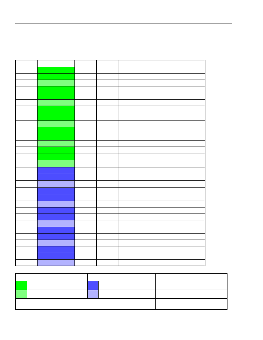
Electrical/Optical Characteristics
Maximum and minimum values are specified over operating case temperature range at 50% duty cycle.
* Note that LVTTL input and output values are different. Input values take board signal losses into consideration.
Table 8. Receiver Electrical I/O Characteristics (Tc = 0 ∞C to 65 ∞C)
Parameter
Symbol
Logic
Min
Typ
Max
Unit
Receiver Input Power Monitor
RxPOWMON
Analog
0.8
1
1.2
V/mW
Receiver Input ac Power Monitor
RxSIGMON
Analog
--
TBD
--
V/mV
Clock Recovery Lock Error:
Output High, V
OH
Output Low, V
OL
RxLOCKERR
LVTTL
2.4
0
--
--
3.47
0.8
V
V
Select MCLK (155 MHz/622 MHz):
Input High, V
IH
Input Low, V
IL
RxMCLKSEL
LVTTL*
2.1
0
--
--
3.47
0.8
V
V
Select Reference Clock:
Input High, V
IH
Input Low, V
IL
RxREFSEL
LVTTL*
2.1
0
--
--
3.47
0.8
V
V
Mute Parallel Output Clock:
Input High, V
IH
Input Low, V
IL
RxMUTEPOCLK
LVTTL*
2.1
0
--
--
3.47
0.8
V
V
Reset:
Input High, V
IH
Input Low, V
IL
RXRESET
LVTTL*
2.1
0
--
--
3.47
0.8
V
V
Rate Select:
Input High, V
IH
Input Low, V
IL
RxRATESEL[1:0]
LVTTL*
2.1
0
--
--
3.47
0.8
V
V
Rx Mute Data Out:
Input High, V
IH
Input Low, V
IL
RxMUTE D
OUT
LVTTL*
2.1
0
--
--
3.47
0.8
V
V
Parallel Data Outputs:
Output High, V
OH
Output Low, V
OL
Differential Output Voltage Swing
RxD
OUT
[15:0]P/N
LVDS
--
0.925
250
--
--
--
1.475
--
400
V
V
mVp-p
Reference Clock Input:
Input Voltage
Frequency Tolerance
Input Duty Cycle
Rise and Fall Times (20%--80%)
RxREFCLKP/N
Differential
ac-coupled
LVDS
100
≠20
40
100
--
--
50
--
400
20
60
TBD
mVp-p
ppm
%
ps
155 MHz Clock Output:
Output High, V
OH
Output Low, V
OL
Output Voltage Swing
Duty Cycle
RxMCLKP/N
LVDS
--
0.925
250
40
--
--
--
50
1.475
--
400
60
V
V
mVp-p
%
Recovered Parallel Output Clock:
Output High, V
OH
Output Low, V
OL
Output Voltage Swing
Duty Cycle
RxPOCLKP/N
LVDS
--
0.925
250
40
--
--
--
50
1.475
--
400
60
V
V
mVp-p
%

24
For additional information and latest specifications, see our website: www.triquint.com
TB64-Type 10 Gb/s Lightwave Transponder
Data Sheet
with 16-Ch. 622 Mb/s MUX/DeMUX and Selectable FEC Rate
March 2003
Electrical/Optical Characteristics
(continued)
Maximum and minimum values are specified over operating case temperature range at 50% duty cycle.
Table 9. Transmitter Electrical I/O Characteristics (T
C
= 0 ∞C to 65 ∞C)
Parameter
Symbol
Logic
Min
Typ
Max
Unit
Laser Enable:
1
Input High, V
IH
Input Low, V
IL
L
S
ENABLE
LVTTL
2
2.1
0
--
--
3.47
0.8
V
V
Laser Bias Output
L
S
BIASMON
Analog
0
500
2500
mV
Laser Degrade Alarm Output:
3
Output High, V
OH
Output Low, V
OL
L
S
BIASALM
LVTTL
2.4
0
--
--
3.47
0.5
V
V
Laser Power Monitor Output
L
S
POWMON
Analog
400
500
600
mV
Lock Error of MUX PLL:
4
Output High, V
OH
Output Low, V
OL
T
X
LOCKERR
LVTTL
2.4
0
--
--
3.47
0.8
V
V
Reference Clock:
Differential Input Voltage Swing
Frequency Tolerance
Input Duty Cycle
Rise and Fall Times (20%--80%)
T
X
REFCLKP/N
Differential
ac-coupled
LVDS
100
≠20
40
100
--
--
50
--
400
20
60
TBD
mVp-p
ppm
%
ps
Input Data Signal Level:
Input Voltage Range
Differential Input Voltage Swing
Differential Input Impedance
T
X
D
IN
[15:0]P/N
LVDS
0
100
80
1200
--
100
2400
400
120
mV
mVp-p
Parallel Input Clock:
Frequency
Input Common Voltage Range
Differential Input Voltage Swing
Differential Input Impedance
T
X
PlCLKP/N
LVDS
--
0
100
80
622.08
1200
--
100
--
2400
400
120
MHz
mV
mVp-p
622 MHz Parallel Output Clock:
Output High, V
OH
Output Low, V
OL
Differential Output Voltage Swing
Duty Cycle
T
X
PCLKP/N
LVDS
--
0.925
250
40
--
--
--
50
1.475
--
400
60
V
V
mVp-p
%
155 MHz Output Clock:
Output High, V
OH
Output Low, V
OL
Diff. Output Voltage Swing
Duty Cycle
T
X
MCLKP/N
LVDS
--
0.925
250
40
--
--
--
50
1.475
--
400
60
V
V
mV
%
1. The transmitter is normally enabled and requires only an active-high external voltage to disable.
2. Please note that LVTTL input and output values are different. Input values take board signal losses into consideration.
3. The alarm will go active-low when the bias current to the laser increases by 50% or decreases by 50% from its beginning-of-life (BOL)
value.
4. Active-low.

For additional information and latest specifications, see our website: www.triquint.com
25
Data Sheet
March 2003
TB64-Type 10 Gb/s Lightwave Transponder
with 16-Ch. 622 Mb/s MUX/DeMUX and Selectable FEC Rate
1. The transmitter is normally enabled and requires only an active-high external voltage to disable.
2. Please note that LVTTL input and output values are different. Input values take board signal losses into consideration.
3. The alarm will go active-low when the bias current to the laser increases by 50% or decreases by 50% from its beginning-of-life (BOL)
value.
4. Active-low.
5. Open-drain output.
T
X
REFCLK
Reference Select:
Input High, V
IH
Input Low, V
IL
T
X
REFSEL
LVTTL
2
2.1
0
--
--
3.47
0.8
V
V
Tx Loss of Lock:
Output High, V
OH
Output Low, V
OL
TxLOCKERR
LVTTL
2.4
0
--
--
3.47
0.8
V
V
Diagnostic Loop Enable:
Input High, V
IH
Input Low, V
IL
RxDLOOPENB
LVTTL
2
2.1
0
--
--
3.47
0.8
V
V
Tx Reset:
Input High, V
IH
Input Low, V
IL
TxRESET
LVTTL
2
2.1
0
--
--
3.47
0.8
V
V
Alarm Interrupt:
Output High, V
OH
Output Low, V
OL
ALMINT
LVTTL
5
2.4
0
--
--
3.47
0.8
V
V
Tx Rate Select:
Input High, V
IH
Input Low, V
IL
TxRATESEL[1:0]
LVTTL
2
2.1
0
--
--
3.47
0.8
V
V
Table 9. Transmitter Electrical I/O Characteristics (T
C
= 0 ∞C to 65 ∞C) (continued)
Parameter
Symbol
Logic
Min
Typ
Max
Unit
Electrical/Optical Characteristics
(continued)
Maximum and minimum values are specified over operating case temperature range at 50% duty cycle.

For additional information and latest specifications, see our website: www.triquint.com
26
Data Sheet
TB64-Type 10 Gb/s Lightwave Transponder
March 2003
with 16-Ch. 622 Mb/s MUX/DeMUX and Selectable FEC Rate
Electrical/Optical Characteristics
(continued)
Maximum and minimum values are specified over operating case temperature range at 50% duty cycle.
Table 10. OC-192/STM-64 Transmitter Optical Characteristics (Tc = 0 ∞C to 65 ∞C)
1. Output power definitions and measurements per ITU-T Recommendation G.691.
2. Full spectral width measured 20 dB down from the central wavelength peak under fully modulated conditions.
3. Ratio of the average output power in the dominant longitudinal mode to the power in the most significant side mode under fully
modulated conditions.
4. Ratio of logic 1 output power to logic 0 output power under fully modulated conditions.
5. Draft ITU-T Recommendation G.693, Optical Interfaces for Intraoffice Systems.
6. GR-253-CORE, Synchronous Optical Network (SONET) OC-192 Transport Systems: Common Generic Criteria.
7. Draft ITU-T Recommendation G.691, Optical Interfaces for Single-Channel SDH Systems with Optical Amplifiers, and STM-64
Systems.
Table 11. OC-192/STM-64 Receiver Optical Characteristics (Tc = 0 ∞C to 65 ∞C)
1. PIN receiver at 1310 nm, 1 x 10
≠12
BER, 2
23
≠ 1 pseudorandom data input.
Parameter
Symbol
Min
Typ
Max
Unit
Average Output Power
1
P
O
≠6
--
≠1
dBm
Operating Wavelength
1290
1310
1330
nm
Spectral Width
2
--
--
--
1
nm
Side-mode Suppression Ratio (DFB laser)
3
SMSR
30
--
--
dB
Extinction Ratio
4
ER
6
--
--
dB
Optical Rise/Fall Times (20%--80%)
t
R
/t
F
--
--
TBD
ps
Optical Path Penalty
P
P
--
--
1
dB
Eye Mask of Optical Output
5
Compliant with ITU-T G.693
Jitter Generation
6, 7
Compliant with GR-253-CORE and ITU-T G.691
Jitter Transfer
6, 7
Compliant with GR-253-CORE and ITU-T G.691
Jitter Tolerance
6, 7
Compliant with GR-253-CORE and ITU-T G.691
Parameter
Symbol
Min
Typ
Max
Unit
Average Receiver Sensitivity (EOL)
1
PR
MIN
≠12
--
--
dBm
Average Receiver Overload (EOL)
--
≠1
--
--
dBm
Receiver Reflectance
--
--
--
≠27
dB
Table 12. Power Supply Characteristics (T
C
= 0 ∞C to 65 ∞C)
Parameter
Symbol
Min
Typ
Max
Unit
3.3 V Supply Voltage
V
DD
3.13
3.3
3.46
V
Supply Current Drain with Internal Reference
Clock Filter
I
DD
1100
1350
1600
mA
Supply Current Drain without Internal Reference
Clock Filter
I
DD
1100
1150
1300
mA
5. 0 V Supply Voltage
V
CC
4.75
5.0
5.25
V
Supply Current Drain
I
CC
100
250
300
mA
≠5. 2 V Supply Voltage
V
EE
≠4.94
≠5.2
≠5.46
V
Supply Current Drain
I
EE
20
100
200
mA
Package Power Dissipation with Internal
Reference Clock Filter
P
DISS
4.6
6.5
8.0
W
Package Power Dissipation without Internal
Reference Clock Filter
P
DISS
4.6
5.6
7.0
W

Data Sheet
March 2003
TB64-Type 10 Gb/s Lightwave Transponder
with 16-Ch. 622 Mb/s MUX/DeMUX and Selectable FEC Rate
For additional information and latest specifications, see our website: www.triquint.com
27
Functional Description
Receiver
The optical receiver in the TB64-type transponder is
optimized for the particular SDH/SONET application
segment in which it was designed to operate and will
have a PIN photodetector. The detected serial data
output of the optical receiver is connected to a clock
and data recovery circuit (CDR) that extracts a
9953.28 MHz clock signal for normal OC-192/STM-64
rate or 10.6642 GHz or 10.709 GHz at FEC rate. This
recovered serial bit clock signal and a retimed serial
data signal are presented to the 16-bit serial-to-parallel
converter.
The receiver contains a lock-detect circuit that monitors
the integrity of the serial data inputs. If the received
serial data fails the frequency test, the PLL will be
forced to lock to the local reference clock. This will
maintain the correct frequency of the recovered clock
output under loss-of-signal or loss-of-power conditions.
Figure 4. TB64-Type Transponder Receiver Timing Characteristics
Table 13. TB64-Type Transponder Receiver Timing Characteristics
Parameter
Symbol
Min
Typ
Max
Unit
Clock Period
T0
--
1.608
--
ns
Duty Cycle
TW/T0
40
50
60
%
Rise/Fall Time (20%--80%)
t
R
/t
F
--
--
300
ps
Data/Clock Skew
T
CQ-MIN/
T
CQ-MAX
--
--
250/250
ps
RxPOCLKP
RxDOUTP/N
V
CROSS
T
CQ_MIN
T
CQ_MAX
V
CROSS
V
CROSS
DATA INVALID WINDOW
T0
TW
V
SWING
1-1283F
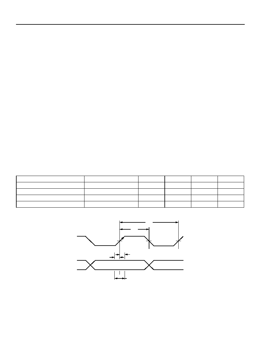
Data Sheet
March 2003
TB64-Type 10 Gb/s Lightwave Transponder
with 16-Ch. 622 Mb/s MUX/DeMUX and Selectable FEC Rate
28
For additional information and latest specifications, see our website: www.triquint.com
Functional Description
(continued)
Transmitter
The optical transmitter in the TB64-type transponder is
optimized for the particular SDH/SONET segment in
which it is designed to operate. The transmitter has an
uncooled direct-modulated laser as the optical element
and operates at the 1310 nm window. A serial data
stream developed in the parallel-to-serial conversion
logic input drives the transmitter.
The parallel-to-serial converter block shown in Figure 1
is comprised of two byte-wide registers. The first regis-
ter latches the 16 bits of parallel input data
(TxDin[15:0]) on the rising edge of TxPICLK. The sec-
ond register is a 16-bit parallel load, serial-out shift reg-
ister that is loaded from the input register. An internally
generated byte clock, which is phase aligned to the
9953.28 MHz serial transmit clock, activates the data
transfer between the input register and the parallel-to-
serial register.
The clock-divider and phase-detect circuitry shown in
Figure 1 generates internal reference clocks and timing
functions for the transmitter. Therefore, it is important
that the TxREFCLKP/N input is generated from a pre-
cise and stable source. It is required that the TxREF-
CLKP/N input be generated from a crystal oscillator or
other source having a frequency accuracy better than
±20 ppm.
The timing generation circuitry provides two separate
functions. One is a byte-rate clock that is synchronized
to the 9953.28 MHz transmit serial clock, the other is a
mechanism for aligning the phase between the incom-
ing byte clock (TxPICLKP/N) and the clock that loads
the parallel data from the input register into the parallel-
to-serial shift register. The TxPCLKP/N output is a
byte-rate (622 MHz) version of the serial transmit clock
and is intended for use by upstream multiplexing and
overhead processing circuits. Using TxPCLKP/N for
upstream circuits will ensure a stable frequency and
phase relationship between the parallel data coming
into the transmitter and the subsequent parallel-to-
serial timing functions.
Figure 5. TB64-Type Transponder Transmitter Timing Characteristics
Table 14. TB64-Type Transponder Transmitter Timing Characteristics
Parameter
Symbol
Min
Typ
Max
Unit
Clock Period
T0
--
1.608
--
ns
Duty Cycle
TW/T0
40
--
60
%
Rise/Fall Time (20%--80%)
t
R
/t
F
100
--
300
ps
Setup Time/Hold Time
T
SETUP/
T
HOLD
--
--
300/300
ps
TxPICLKP
TxDINP/N
V
CROSS
T
SETUP
T
HOLD
V
CROSS
V
CROSS
DATA VALID WINDOW
T0
TW
1-1284F

Data Sheet
March 2003
TB64-Type 10 Gb/s Lightwave Transponder
with 16-Ch. 622 Mb/s MUX/DeMUX and Selectable FEC Rate
For additional information and latest specifications, see our website: www.triquint.com
29
Transponder Interfacing
Receiver Interface Board Layout
All the receiver data outputs (RxD
OUT
P/N[15:0]) on the
customer board should have equal trace lengths, and
in most cases, be matched to that of the parallel output
clock RxPOCLKP/N. The similar lengths ensure that
these signals maintain the propagation delay time val-
ues.
It is not required to match the trace length of the
RxMCLKP/N. RxMCLKP/N is derived from the RxREF-
CLKP/N, i.e., from a VCO inside the deMUX. This
allows a clock signal to be delivered to the framer even
if the RxPOCLKP/N is not locked to any incoming opti-
cal signal.
Figure 6 shows the TB64 receiver interface board lay-
out
Note: RxMCLKP/N may not be required for all framers.
Figure 6. TB64-Type Receiver Interface Board Layout
DeMUX IC
RxDOUTP/N[15:0]
622 Mb/s
RxPOCLKP/N
RxMCLKP/N
622 MHz
TRACES MUST BE THE SAME LENGTH
OSCILLATOR
RxREFCLKP/N
155 MHz
622 MHz
100 ppm
CUSTOMER
BOARD
FRAMER IC
1-1136F

Data Sheet
March 2003
TB64-Type 10 Gb/s Lightwave Transponder
with 16-Ch. 622 Mb/s MUX/DeMUX and Selectable FEC Rate
30
For additional information and latest specifications, see our website: www.triquint.com
Transponder Interfacing
(continued)
Transmitter Interface Board Layout
All the transmitter data inputs, (TxD
IN
P/N[15:0]) should
have equal trace lengths on the customer board. There
should also be a certain phase relationship between
TxD
IN
P/N[15:0] and the parallel input clock
(TxPICLKP/N) at the transponder electrical connector
input to allow proper MUX operation, as shown by the
setup and hold times (T
SETUP/
T
HOLD
) in Table 14 on
page 28. This phase relationship can be ensured if the
trace length of the TxPICLKP/N is matched to the trace
length of the TxD
IN
P/N data inputs. For TxREFCLKP/N
clock, a tolerance of ±20 ppm is required to meet
SONET output frequency specifications. To ensure
this, using VCXO/PLL circuit is recommended.
The VCO/VCXO chosen should be of an OC-192
SONET quality. The clock should have low phase noise
and frequency stability of better than ±20 ppm.
Figure 7 shows the TB64-type transmitter interface
board layout. Please contact TriQuint Optoelectronics
for more details.
Figure 7. TB64-Type Transmitter Interface Board Layout
TxDINP/N[15:0]
622 Mb/s
TxPICLKP/N
TxPCLKP/N
622 MHz
TRACES SHOULD BE THE SAME LENGTH
TxREFCLKP/N
622 MHz OR 155 MHz
CUSTOMER BOARD
SYSTEM
CLOCK
VCXO/PLL
FRAMER IC
MUX IC
1-1140F
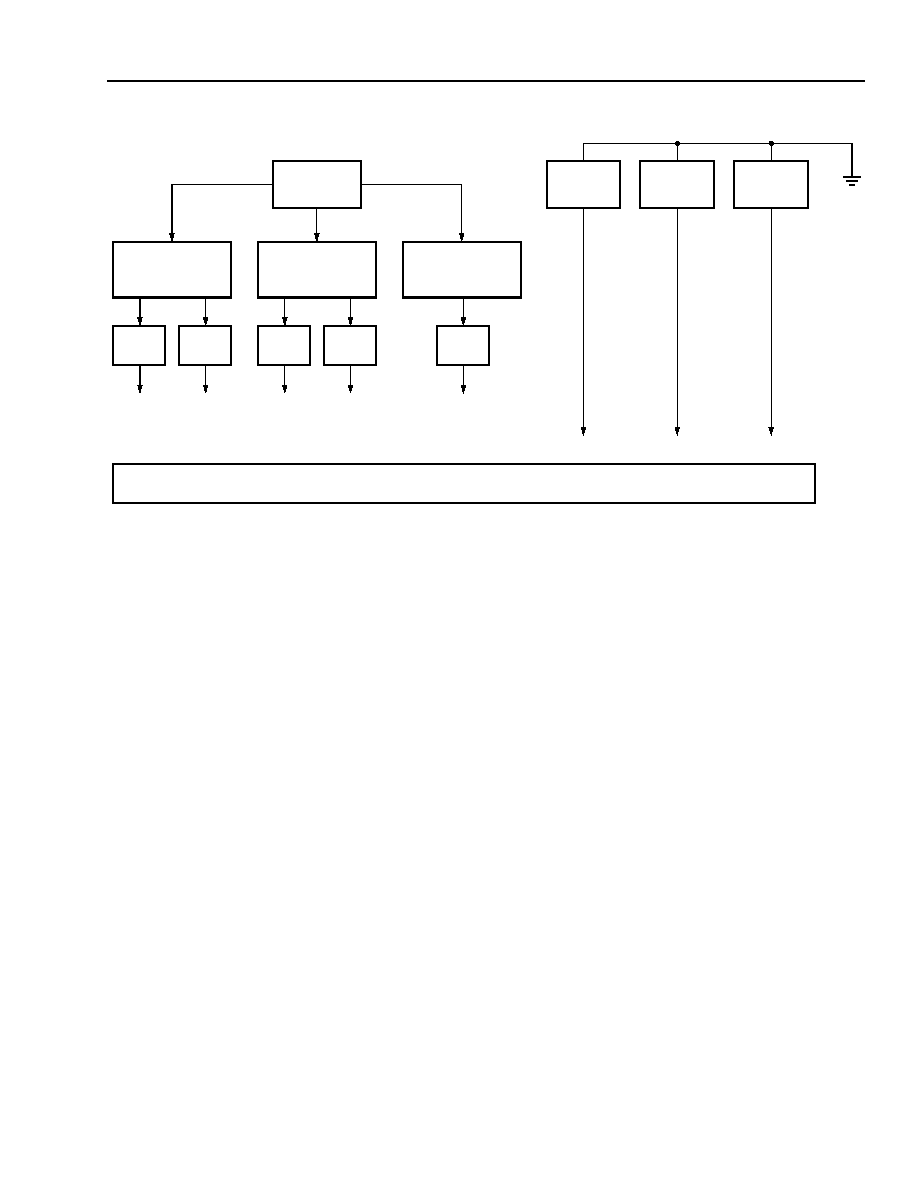
For additional information and latest specifications, see our website: www.triquint.com
31
Data Sheet
TB64-Type 10 Gb/s Lightwave Transponder
March 2003
with 16-Ch. 622 Mb/s MUX/DeMUX and Selectable FEC Rate
Transponder Grounding
Figure 8. Recommended Grounding Scheme
Qualification and Reliability
To help ensure high product reliability and customer satisfaction, TriQuint Optoelectronics is committed to an inten-
sive quality program that starts in the design phase and proceeds through the manufacturing process. Optoelec-
tronics modules are qualified to our internal standards using MIL-STD-883 test methods and procedures and using
sampling techniques consistent with Telcordia Technologies TM requirements. This qualification program fully
meets the intent of Telcordia Technologies reliability practices TR-NWT-000468 for optoelectronic parts, and the
transponder as a subsystem meets NEBS GR63-CORE requirements. In addition, our design, development, and
manufacturing facility has been certified to be in full compliance with the latest ISO
Æ
9001 quality system stan-
dards.
48 Vdc
dc-TO-dc
CONVERTER
FILTER
FILTER
dc-TO-dc
CONVERTER
dc-TO-dc
CONVERTER
FILTER
FILTER
FILTER
DIGITAL
GROUND
ANALOG
GROUND
TRANSPONDER
≠5.2 V
ANALOG
≠5.2 V
DIGITAL
3.3 V
ANALOG
3.3 V
DIGITAL
5.0 V
ANALOG
50 mV PK-TO-PK NOISE MAX ON ALL POWER SUPPLY OUTPUTS
FRAME
GROUND
1-1317F

32
For additional information and latest specifications, see our website: www.triquint.com
TB64-Type 10 Gb/s Lightwave Transponder
Data Sheet
with 16-Ch. 622 Mb/s MUX/DeMUX and Selectable FEC Rate
March 2003
Electrostatic Discharge
CAUTION: This device is susceptible to damage as a result of electrostatic discharge. Take proper precau-
tions during both handling and testing. Follow guidelines such as JEDEC Publication No. 108-A
(Dec. 1988).
TriQuint employs a human-body model (HBM) for ESD-susceptibility testing and protection-design evaluation. ESD
voltage thresholds are dependent on the critical parameters used to define the model. A standard HBM (resistance
= 1.5 k
, capacitance = 100 pF) is widely used and can be used for comparison purposes.
Regulatory and Voluntary Compliance
*Complies with applicable Telcordia NEBS Level 1--3 EMC requirements for components in a standalone configuration.
CAUTION: Use of controls, adjustments, and procedures other than those specified herein may result in
hazardous laser radiation exposure.
NOTICE
Unterminated optical connectors can emit laser radiation.
Do not view with optical instruments.
Table 15. Regulatory and Voluntary Compliance
Feature
Standard
Test Parameters/Performance
Electrostatic Discharge (ESD) to
the Electrical Pins
Sensitivity Classification:
MIL-STD-883E, Method 3015.7
Class 1 (0V to 1,999V)
Electrostatic Discharge (ESD) to
Housing and Optical Connector
EN 61000-4-2, IEC
Æ
61000-4-2
Full recovery following ±8 kV contact
discharge and ±15 kV air discharge
Electromagnetic Compatibility:
Radiated Emissions
Immunity
FCC Part 15, Class B
EN55022, Class B
GR-1089_CORE*
EN 61000-4-3
GR-1089_CORE*
Full compliance within the frequency
range of 10 KHz--20 GHz
Full compliance within the frequency
range of 10 KHz--10 GHz at a field
strength of 8.5 V/m
Safety of Information Technology
Equipment
IEC 60950
EN 60950
UL
Æ
60950
CAN/CSA
Æ
-C22.2 No. 60950
CB Scheme:
Test Report Reference
No. 01RT14477-02252002,
Reference Certificate
No. US/5754/UL,
UL/CSA Recognition File
No. E225949
Laser Safety
21 CFR 1040.10 and 1040.11,
includes Laser Notice No. 50,
IEC 60825-1:1993,
A1:1997, and A2:2001
CDRH Accession No.
(872009-59)
AEL Class 1
CE Mark
LVD 73/23/EEC
EMC 89/336/EEC
EC Declaration of Conformity
Component Recognition
UL and CSA Joint Component Rec-
ognition for Information Technology
Equipment
UL File Number:
E225949
Compositional Analysis
Standard ICPS, GC/MS, FTIR
Analytical Processes
Analytical test results:
elements, organic compounds
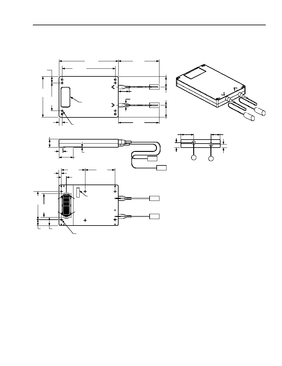
For additional information and latest specifications, see our website: www.triquint.com
33
Data Sheet
TB64-Type 10 Gb/s Lightwave Transponder
March 2003
with 16-Ch. 622 Mb/s MUX/DeMUX and Selectable FEC Rate
Outline Diagram
Dimensions are in inches and (millimeters).
Notes:
Compact size of 3.6 in. x 2.6 in. x 0.53 in.
Package properties:
-- Material: aluminum alloy 6061-T6 per QQ-A-250/11.
-- Finish: clear chromate (conductive) per MIL-C-5541, Class 3.
Four M2.5 threaded holes are to mount the transponder on the customer board:
--Transponder mounting holes (bottom cover): maximum screw depth = 0.080 in. (2.00 mm) (thread 0.080 in. [2 mm] deep).
Four M2.5 threaded holes are for possible mounting of an external heat sink:
-- External heat sink mounting holes (top cover): maximum screw depth = 0.100 in. (2.54 mm) (thread 0.100 in. [2.54 mm] deep).
TriQuint Optoelectronics recommends that customers use a 300-pin plug FCI Berg #84500-102 (30 min gold plated) that meets Telcordia
Technologies' 100 insertions criterion.
TriQuint Optoelectronics also recommends that the distance between the Berg connector center-line and the nearest customer compo-
nents behind the transponder be 0.8 in. minimum to ensure that future transponders are accommodated without any board layout change.
The pigtails are 1 meter ± 10 cm in length (39.4 in. ± 3.9 in.) as specified by dimension X in Figure 9. A yellow sleeve UL
Æ
-approved (TBD, 94V-
2) jacket is placed at the receiver end of the pigtail.
Figure 9. Mechanical Dimensions
1-1142 (F)c2
UNSPECIFIED TOLERANCES:
ONE PLACE, ±0.1
TWO PLACES, ±0.01
THREE PLACES, ±0.003
FOUR PLACES, ±0.0005
ANGULAR, ±1.0
∞
3.600
(91.44)
2.600
(66.04)
0.530
(13.46)
0.015
(0.38)
PIN A30
PIN A1
1.800
(45.72)
1.840
(46.74)
(6X) M2.5 MOUNTING HOLES
0.370
(9.40)
0.934
(23.72)
1.000
(25.42)
PIN K30
PIN K1
0.305
(7.75)
0.213
(5.41)
RECEIVER
1.975
(50.17)
0.312
(7.92)
0.140
(3.56)
0.240
(6.10)
(4X) M2.5 THREADED
0.768
(19.51)
1.705
(43.31)
0.448
(11.37)
HEATSINK MOUNTING HOLES
1.170
(29.72)
0.662
(16.81)
1.530
(38.86)
SERIAL NUMBER
LABEL
DIM "X"
DIM "X"
0.380
(9.65)
0.662
(16.81)
0.768
(19.51)
TRANSMITTER
CODE LABEL
ÿ 0.260
(6.60)
3.320
(84.33)
0.130
(3.30)

Additional Information
For the latest specifications, additional product information, worldwide sales and distribution locations, and information about TriQuint:
Web: www.triquint.com
Tel: (503) 615-9000
E-mail: info_opto@tqs.com
Fax: (503) 615-8902
For technical questions and additional information on specific applications:
E-mail: info_opto@tqs.com
The information provided herein is believed to be reliable; TriQuint assumes no liability for inaccuracies or omissions. TriQuint assumes no responsibility for the use of this information, and all
such information shall be entirely at the user's own risk. Prices and specifications are subject to change without notice. No patent rights or licenses to any of the circuits described herein are
implied or granted to any third party.
TriQuint does not authorize or warranty any TriQuint product for use in life-support devices and/or systems.
Copyright © 2003 TriQuint Semiconductor Inc. All rights reserved.
DS03-012 (Replaces DS02-087), March, 2003
Data Sheet
March 2003
TB64-Type 10 Gb/s Lightwave Transponder
with 16-Ch. 622 Mb/s MUX/DeMUX and Selectable FEC Rate
Ordering Information
Table 16. Ordering Information
Device Description
Reference Clock
Filter
Connector
Type
2km Reach
12km Reach
Device Code
Comcode
Device Code
Comcode
No Filter
SC
TB64M1CAA
700006729
TB64N1CAA
109142125
LC
TB64M1WAA
700016314
TB64N1WAA
700016282
622 MHz VCO
SC
TB6AM1CAA
700006731
TB6AN1CAA
109144097
LC
TB6AM1WAA
700016325
TB6AN1WAA
700016288
155 MHz VCO
SC
TB6BM1CAA
700006732
TB6BN1CAA
109142133
LC
TB6BM1WAA
700016328
TB6BN1WAA
700016294
666 MHz VCO
SC
TB6CM1CAA
700006733
TB6CN1CAA
109142141
LC
TB6CM1WAA
700016333
TB6CN1WAA
700016301
166 MHz VCO
SC
TB6DM1CAA
700006734
TB6DN1CAA
109142158
LC
TB6DM1WAA
700016336
TB6DN1WAA
700016307
Telcordia Technologies is a trademark of Telcordia Technologies, Inc.
ISO is a registered trademark of The International Organization for Standardization.
IEC is a registered trademark of The International Electrotechnical Commission.
UL is a registered trademark of Underwriters Laboratories, Inc.