TriQuint Semiconductor Texas: (972)994 8465 Fax (972)994 8504 Web: www.triquint.com
Product Data Sheet
1
December 13, 2001
36 to 40 GHz 1W Power Amplifier TGA1171-SCC
Key Features and Performance
�
0.25 um pHEMT Technology
�
36-40 GHz Frequency Range
�
29 dBm Nominal Pout @ P1dB, 38 GHz
�
14 dB Nominal Gain
�
OTOI 36 dBm at 40 GHz typical
�
Bias 6-7 V @ 500 mA
�
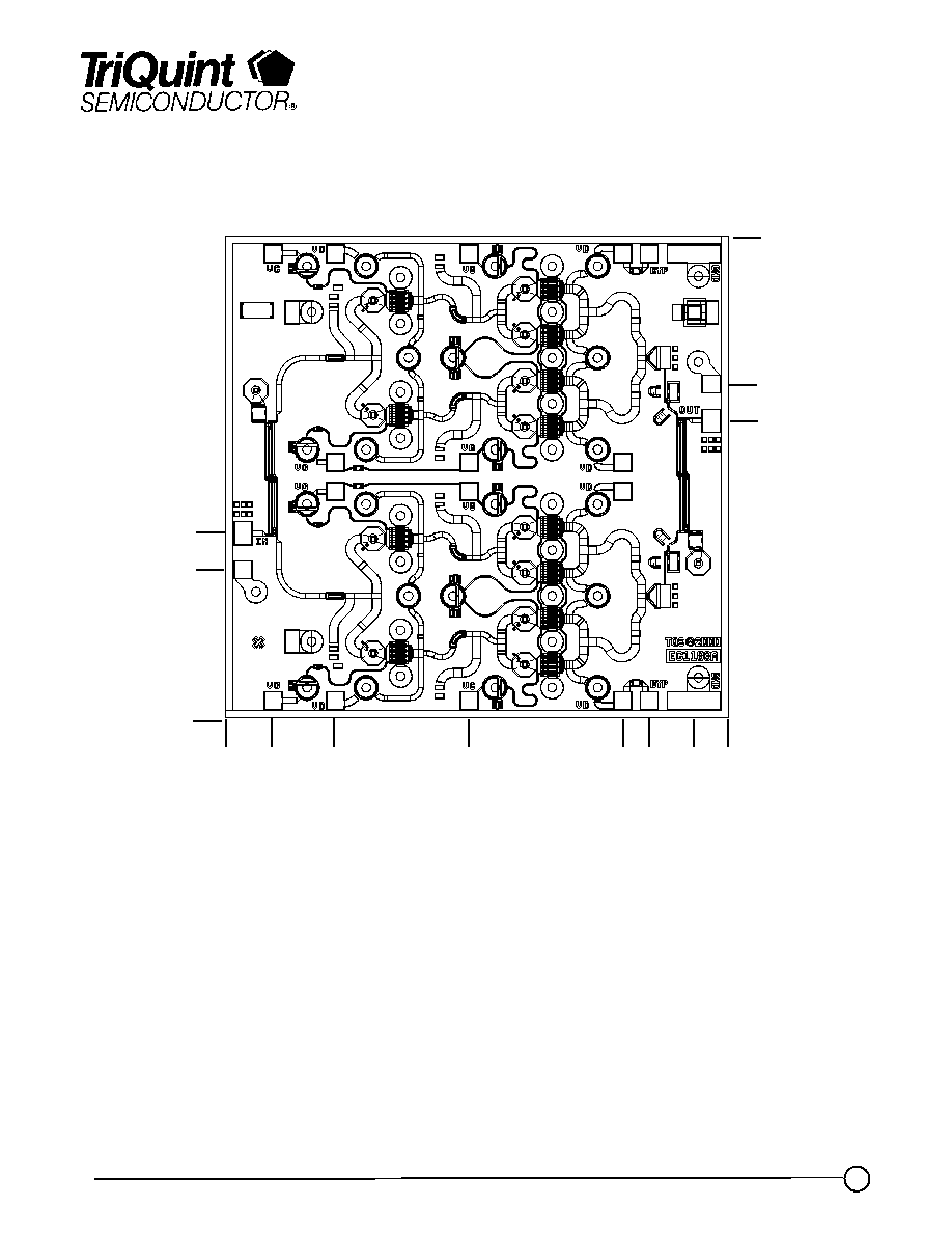
Chip Dimensions: 2.863 mm x 2.740 mm
x 0.1016 mm
Primary Applications
�
Point-to-Point Radio
�
Point-to-Multipoint Radio
Product Description
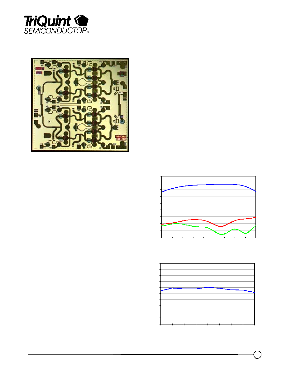
The TriQuint TGA1171-SCC is a two-stage
PA MMIC design using TriQuint's proven 0.25
�
m Power pHEMT process to support a
variety of millimeter wave applications
including point-to-point digital radio and point-
to-multipoint systems.
The balanced design consists of four 400
�
m
input devices driving eight 400
�
m output
devices.
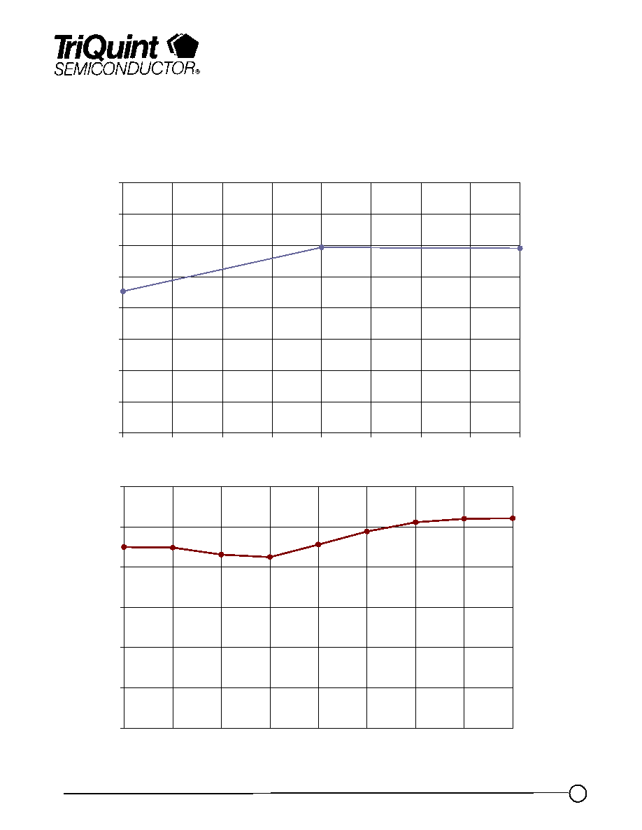
The TGA1171 provides 29 dBm of output
power at 1 dB gain compression and >30
dBm saturated output power across 36-40
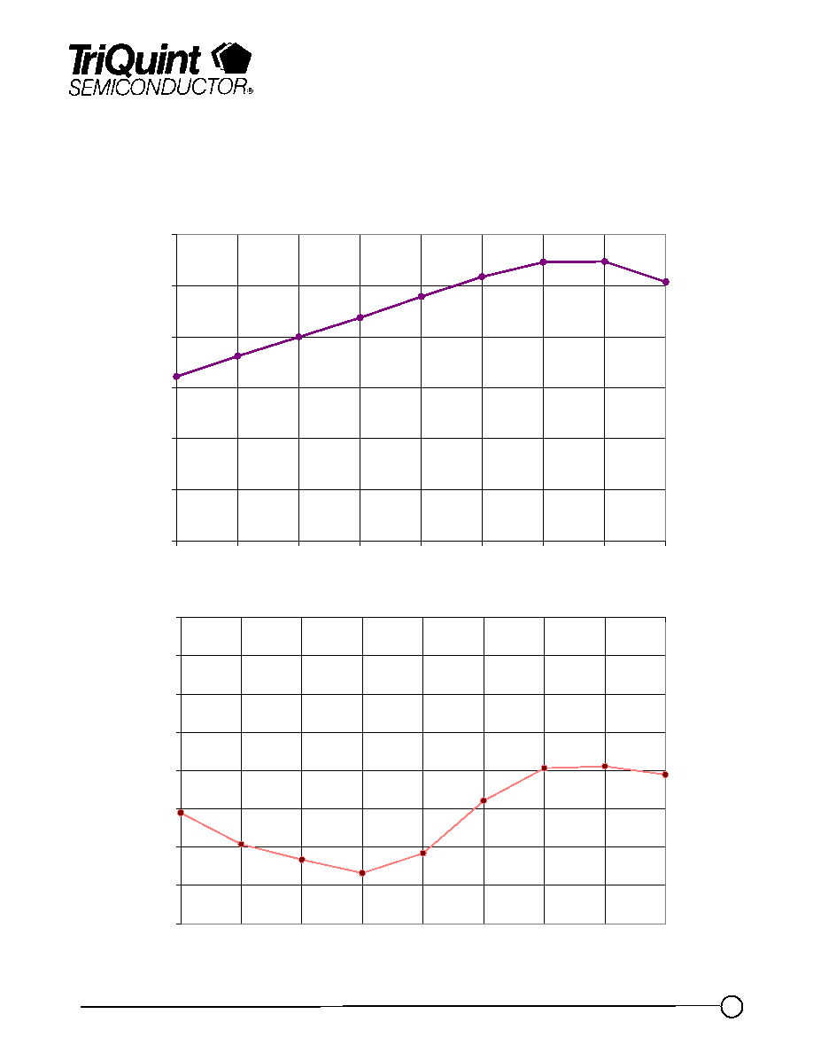
GHz with a typical small signal gain of 14 dB.
Typical Input/Output RL is typically greater
than 12-15 dB across the band.
The TGA1171 requires minimal off-chip
components. Each device is 100% DC and
RF tested on-wafer to ensure performance
compliance. The device is available in chip
form.
TGA1171 Fixture Data
+7V, 500mA, 25C
24
25
26
27
28
29
30
31
32
33
34
36.0
36.5
37.0
37.5
38.0
38.5
39.0
39.5
40.0
Frequency (GHz)
Out
put
P1
dB (
d
Bm)
TGA1171 Fixture Data
+7V, 500mA, 25C
-25
-20
-15
-10
-5
0
5
10
15
20
33
34
35
36
37
38
39
40
41
42
Frequency (GHz)
Ga
i
n
a
n
d
Re
t
u
r
n
L
o
s
s
(
d
B)
S21
S11
S22

TriQuint Semiconductor Texas: (972)994 8465 Fax (972)994 8504 Web: www.triquint.com
Product Data Sheet
2
December 13, 2001
TABLE I
MAXIMUM RATINGS
Symbol
Parameter 5/
Value
Notes
V
+
Positive Supply Voltage
8 V
4/
V
-
Negative Supply Voltage Range
-5V TO 0V
I
+
Positive Supply Current (Quiescent)
9 6 0 mA
4/
| I
G
|
Gate Supply Current
56.32 mA
P
IN
Input Continuous Wave Power
27 dBm
4/
P
D
Power Dissipation
5.25 W
3/ 4/
T
CH
Operating Channel Temperature
150
0
C
1/ 2/
T
M
Mounting Temperature
(30 Seconds)
320
0
C
T
STG
Storage Temperature
-65 to 150
0
C
1/
These ratings apply to each individual FET.
2/
Junction operating temperature will directly affect the device median time to failure (T
M
).
For maximum life, it is recommended that junction temperatures be maintained at the
lowest possible levels.
3/
When operated at this bias condition with a base plate temperature of 70
0
C, the median
life is reduced from 9.5 E+6 to 6.1 E+5 hours.
4/
Combinations of supply voltage, supply current, input power, and output power shall not
exceed P
D
.
5/
These ratings represent the maximum operable values for this device.
TGA1171-SCC

TriQuint Semiconductor Texas: (972)994 8465 Fax (972)994 8504 Web: www.triquint.com
Product Data Sheet
3
December 13, 2001
TABLE II
DC PROBE TEST
(TA = 25
�
C
�
5
�
C)
Symbol
Parameter
Minimum
Maximum
Unit
Idss
(Q3-6)
Saturated Drain Current
160
752
mA
Gm
(Q3-6)
Transconductance
352
848
mS
V
P
Pinch-off Voltage
-1.5
-0.5
V
BVGS
(Q3-6)
Breakdown Voltage Gate-
Source
-30
-11
V
BVGD
(Q3-6)
Breakdown Voltage Gate-
Drain
-30
-11
V
TABLE III
AUTOPROBE FET PARAMETER MEASUREMENT CONDITIONS
FET Parameters
Test Conditions
I
DSS
:
Maximum drain current (I
DS
) with gate voltage
(V
GS
) at zero volts.
V
GS
= 0.0 V, drain voltage (V
DS
) is swept from 0.5 V up to
a maximum of 3.5 V in search of the maximum value of
I
DS
; voltage for I
DSS
is recorded as VDSP.
G
m
: Transconductance;
I
DSS
-
IDS 1
(
)
VG1
For all material types, V
DS
is swept between 0.5 V and
VDSP in search of the maximum value of I
ds
. This
maximum I
DS
is recorded as IDS1. For Intermediate and
Power material, IDS1 is measured at V
GS
= VG1 = -0.5 V.
For Low Noise, HFET and pHEMT material,
V
GS
= VG1 = -0.25 V. For LNBECOLC, use
V
GS
= VG1 = -0.10 V.
V
P
:
Pinch-Off Voltage; V
GS
for I
DS
= 0.5 mA/mm of
gate width.
V
DS
fixed at 2.0 V, V
GS
is swept to bring I
DS
to 0.5 mA/mm.
V
BVGD
:
Breakdown Voltage, Gate-to-Drain; gate-to-drain
breakdown current (I
BD
) = 1.0 mA/mm of gate width.
Drain fixed at ground, source not connected (floating),
1.0 mA/mm forced into gate, gate-to-drain voltage (V
GD
)
measured is V
BVGD
and recorded as BVGD; this cannot be
measured if there are other DC connections between gate-
drain, gate-source or drain-source.
V
BVGS
:
Breakdown Voltage, Gate-to-Source; gate-to-
source breakdown current (I
BS
) = 1.0 mA/mm of gate
width.
Source fixed at ground, drain not connected (floating),
1.0 mA/mm forced into gate, gate-to-source voltage (V
GS
)
measured is V
BVGS
and recorded as BVGS; this cannot be
measured if there are other DC connections between gate-
drain, gate-source or drain-source.
TGA1171-SCC

TriQuint Semiconductor Texas: (972)994 8465 Fax (972)994 8504 Web: www.triquint.com
Product Data Sheet
4
December 13, 2001
TABLE V
THERMAL INFORMATION*
Parameter
Test Conditions
T
CH
(
o
C)
R
JC
(
�
C/W)
T
M
(HRS)
R
JC
Thermal Resistance
(channel to backside of
carrier)
Vd = 7V
I
D
= 500 mA
Pdiss = 3.5 W
125.03
15.79
9.5 E+6
Note: Assumes eutectic attach using 1.5 mil 80/20 AuSn mounted to a 20 mil CuMo Carrier
at 70
�
C baseplate temperature. Worst case condition with no RF applied, 100% of DC
power is dissipated.
* This information is a result of a thermal model analysis.
TABLE IV
RF WAFER CHARACTERIZATION TEST
(T
A
= 25
�
C + 5
�
C)
(Vd = 7V, Id = 500 mA
�
5%)
Parameter
Unit
Min
Typical
Max
Frequency
GHz
36
40
Output P1dB
dBm
26
29
Small Signal Gain
dB
12
14
Input Return Loss
dB
-15
Output Return Loss
dB
-15
Output TOI
dBm
36
TGA1171-SCC

TriQuint Semiconductor Texas: (972)994 8465 Fax (972)994 8504 Web: www.triquint.com
Product Data Sheet
5
December 13, 2001
TGA1171-SCC
24
25
26
27
28
29
30
31
32
36
36.5
37
37.5
38
38.5
39
39.5
40
Frequency (GHz)
Pout
@
P1
dB
(
d
Bm
)
-40
-35
-30
-25
-20
-15
-10
36
36.5
37
37.5
38
38.5
39
39.5
40
Frequency (GHz)
Inp
ut
R
e
t
u
r
n
L
o
s
s
(
d
B
)
Data Based on the 50th percentile On-Wafer RF
Probe Test Results, Sample Size = 13971 Devices
Bias Conditions: Vd = 7 V, Id = 500 mA

TriQuint Semiconductor Texas: (972)994 8465 Fax (972)994 8504 Web: www.triquint.com
Product Data Sheet
6
December 13, 2001
TGA1171-SCC
10
11
12
13
14
15
16
36
36.5
37
37.5
38
38.5
39
39.5
40
Frequency (GHz)
G
a
in (
d
B
)
-26
-24
-22
-20
-18
-16
-14
-12
-10
36
36.5
37
37.5
38
38.5
39
39.5
40
Frequency (GHz)
O
u
t
p
u
t
Re
t
u
rn
L
o
s
s
(
d
B)
Data Based on the 50th percentile On-Wafer RF
Probe Test Results, Sample Size = 13971 Devices
Bias Conditions: Vd = 7 V, Id = 500 mA

TriQuint Semiconductor Texas: (972)994 8465 Fax (972)994 8504 Web: www.triquint.com
Product Data Sheet
7
December 13, 2001
Mechanical Characteristics
Dimensions in mm
RF Pads: 130x100
�
m
DC Pads: 100x100
�
m
Die Area: 7.845 mm
2
0.000
1.050
1.690
0.
0
0
0
0.
6
2
5
1.
3
8
5
2.
2
6
0
2.740
0.
2
7
0
2.
4
1
5
2.
6
6
0
2.
8
6
3
0.840
1.900
TGA1171-SCC
1
1

TriQuint Semiconductor Texas: (972)994 8465 Fax (972)994 8504 Web: www.triquint.com
Product Data Sheet
8
December 13, 2001
Chip Assembly and Bonding Diagram
GaAs MMIC devices are susceptible to damage from Electrostatic Discharge. Proper precautions should
be observed during handling, assembly and test.
.01uF, 2 PL
.01uF, 2 PL
100pF, 2 PL
100pF, 2 PL
Vg
Vd
Vg
Vd
RF in
RF out
Vg
Vd
Vg
Vd
Add additional 1uF on drain bias lines for lab testing
Add additional 1uF on drain bias lines for lab testing
5 chisel bonds
or 3 mil ribbon
2PL
TGA1171-SCC

TriQuint Semiconductor Texas: (972)994 8465 Fax (972)994 8504 Web: www.triquint.com
Product Data Sheet
9
December 13, 2001
Assembly Process Notes
GaAs MMIC devices are susceptible to damage from Electrostatic Discharge. Proper precautions should
be observed during handling, assembly and test.
Reflow process assembly notes:
�
Use AuSn (80/20) solder with limited exposure to temperatures at or above 300
C.
�
An alloy station or conveyor furnace with reducing atmosphere should be used.
�
No fluxes should be utilized.
�
Coefficient of thermal expansion matching is critical for long-term reliability.
�
Devices must be stored in a dry nitrogen atmosphere.
Component placement and adhesive attachment assembly notes:
�
Vacuum pencils and/or vacuum collets are the preferred method of pick up.
�
Air bridges must be avoided during placement.
�
The force impact is critical during auto placement.
�
Organic attachment can be used in low-power applications.
�
Curing should be done in a convection oven; proper exhaust is a safety concern.
�
Microwave or radiant curing should not be used because of differential heating.
�
Coefficient of thermal expansion matching is critical.
Interconnect process assembly notes:
�
Thermosonic ball bonding is the preferred interconnect technique.
�
Force, time, and ultrasonics are critical parameters.
�
Aluminum wire should not be used.
�
Discrete FET devices with small pad sizes should be bonded with 0.0007-inch wire.
�
Maximum stage temperature is 200
C.
TGA1171-SCC
