TriQuint Semiconductor Texas: Phone (972)994-8465 Fax (972)994-8504 Email: Info-mmw@tqs.com Web: www.triquint.com
Advance Product Information
July 15, 2005
1
-30
-20
-10
0
10
20
30
4
5
6
7
8
9
10 11 12 13 14
Frequency (GHz)
S
p
ar
& NF (
d
B)
0
1
2
3
4
5
6
Noi
s
e
Fi
g
ur
e
(
dB
)
-30
-20
-10
0
10
20
30
4
5
6
7
8
9
10 11 12 13 14
Frequency (GHz)
S
p
ar
& NF (
d
B)
0
1
2
3
4
5
6
Noi
s
e
Fi
gur
e
(
d
B)
Product Description
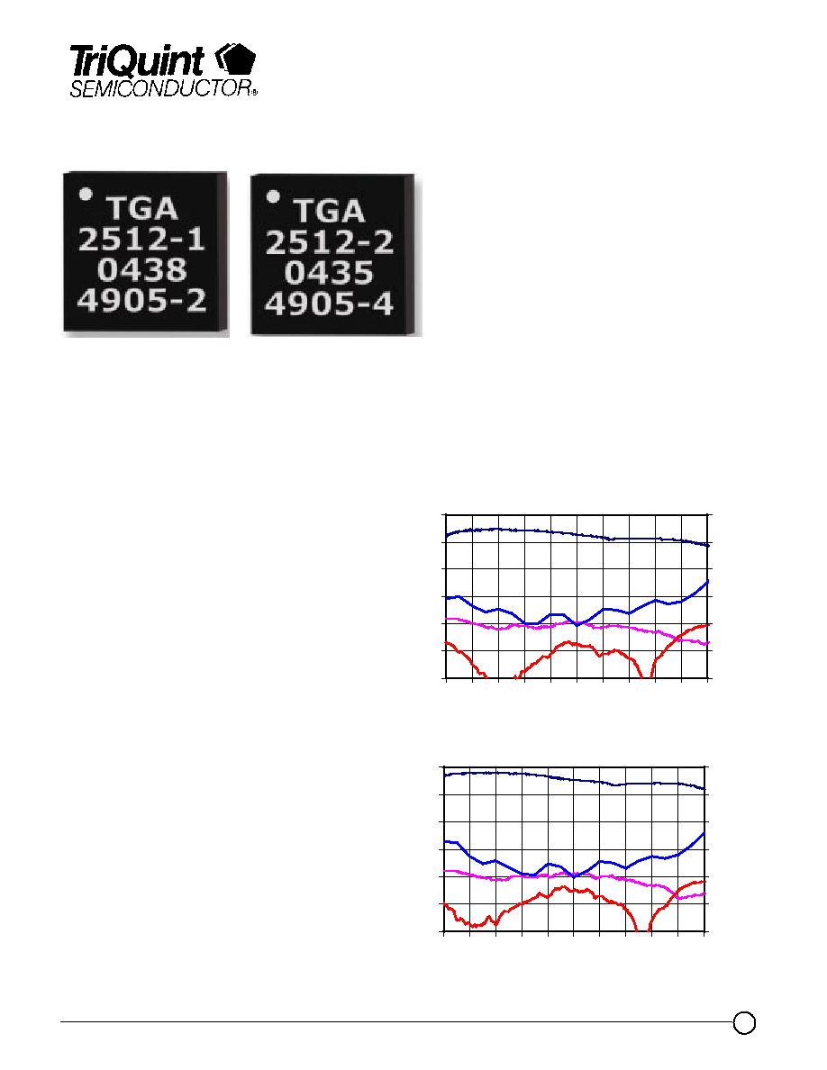
The TriQuint TGA2512-SM is a packaged X-
band balanced LNA with AGC amplifier for EW,
ECM, and RADAR receiver or driver amplifier
applications. The TGA2512-SM provides
excellent noise performance with typical
midband NF of 2.3dB, and high gain, 25dB from
4-14GHz
The TGA2512-SM is designed for maximum
ease of use. TGA2512-SM can handle up to
21dBm input power reliably, while the build-in
gain control provides 15dB of typical gain
control range. The part can be used in self-
biased mode, with a single +5V supply
connection, or in gate biased mode, allowing
the user to control the current for a particular
application.
In self-biased mode the TGA2512-SM achieves
6dBm typical P1dB, while in gate-biased mode
the typical P1dB is over 13dBm.
Lead-Free & RoHS compliant.
Evaluation boards are available.
Primary Applications
�
X-Band Radar
�
EW, ECM
�
Point-to-Point Radio
4 - 14 GHz balanced LNA
TGA2512-SM
Measured Data
ORL
Gain
IRL
Key Features
�
Typical Frequency Range: 4 - 14 GHz
�
2.3 dB Nominal Noise Figure
�
25 dB Nominal Gain
�
15 dB AGC Range
�
13 dBm Nominal P1dB
�
24dBm Nominal OIP3
�
Bias: 5 V, 160 mA Gate Bias
5 V, 90 mA Self Bias
�
Package Dimensions:
4.0 x 4.0 x 0.9 mm
Bias Conditions: Gate Bias, Vd = 5V, Id = 160mA
Bias Conditions: Self Bias, Vd = 5V, Id = 90mA
NF
Gain
NF
ORL
IRL
Self Bias
Gate Bias
Note: Device is early in the characterization process prior to finalizing all electrical specifications. Specifications are subject to change
without notice

TriQuint Semiconductor Texas: Phone (972)994-8465 Fax (972)994-8504 Email: Info-mmw@tqs.com Web: www.triquint.com
Advance Product Information
July 15, 2005
2
TGA2512-SM
TABLE I
MAXIMUM RATINGS 1/
SYMBOL
PARAMETER
VALUE
NOTES
Vd
Drain Voltage
[3.5 + (0.0125)(Id)] V
2/ 3/
Vg
Gate Voltage Range
-1 TO +0.5 V
Id
Drain Current (gate biased)
240 mA
2/
Ig
Gate Current
7.04 mA
P
IN
Input Continuous Wave Power
21 dBm
P
D
Power Dissipation
See note 4/
2/
T
CH
Operating Channel Temperature
117
0
C
5/
T
M
Mounting Temperature (30 Seconds)
260
0
C
T
STG
Storage Temperature
-65 to 150
0
C
T
CASE
Package Operating Temperature
-40 to 110
0
C
1/
These ratings represent the maximum operable values for this device.
2/
Combinations of supply voltage, supply current, input power, and output power shall not exceed P
D
.
3/
Unit for Id is A
4/
For a median life time of 1E+6 hrs, Power dissipation is limited to:
P
D
(max) = (117
0
C � T
BASE
0
C) /
JC
(
0
C/W)
Where T
BASE
is the base plate temperature.
JC
for self bias is 28.2
0
C/W
JC
for gate bias is 37.6
0
C/W
5/
Junction operating temperature will directly affect the device median time to failure (MTTF). For
maximum life, it is recommended that junction temperatures be maintained at the lowest possible
levels.

TriQuint Semiconductor Texas: Phone (972)994-8465 Fax (972)994-8504 Email: Info-mmw@tqs.com Web: www.triquint.com
Advance Product Information
July 15, 2005
3
TABLE II
ELECTRICAL CHARACTERISTICS
(Ta = 25
0
C, Nominal)
TGA2512-SM
PARAMETER
Gate Bias
Self Bias
UNITS
Frequency Range
4 - 14
4 - 14
GHz
Drain Voltage, Vd
5.0
5.0
V
Drain Current, Id
160
90
mA
Gate Voltage, Vg
-0.1
-
V
Small Signal Gain, S21
25
22
dB
Input Return Loss, S11
10
10
dB
Output Return Loss, S22
20
20
dB
Noise Figure, NF
2.3
2.3
dB
Output Power @ 1dB Gain Compression, P1dB
13
6
dBm
OIP3
24
16
dBm
Temperature Gain Coefficent
-0.02
-0.02
dB/
0
C
Note: Table II Lists the RF Characteristics of typical devices as determined by fixtured
measurements.
TABLE III
THERMAL INFORMATION
PARAMETER
TEST CONDITIONS
T
CH
(
O
C)
T
JC
(
q
C/W)
T
M
(HRS)
T
JC
Thermal Resistance
(channel to Case)
Vd = 5 V
Id = 160 mA Gate Bias
Pdiss = 0.80 W
100
37.6
5.8E+6
T
JC
Thermal Resistance
(channel to Case)
Vd = 5 V
Id = 90 mA Self Bias
Pdiss = 0.45 W
82.7
28.2
4.1E+7
Note: Worst case condition with no RF applied, 100% of DC power is dissipated, Case
Temperature @ 70
O
C

TriQuint Semiconductor Texas: Phone (972)994-8465 Fax (972)994-8504 Email: Info-mmw@tqs.com Web: www.triquint.com
Advance Product Information
July 15, 2005
4
TGA2512-SM
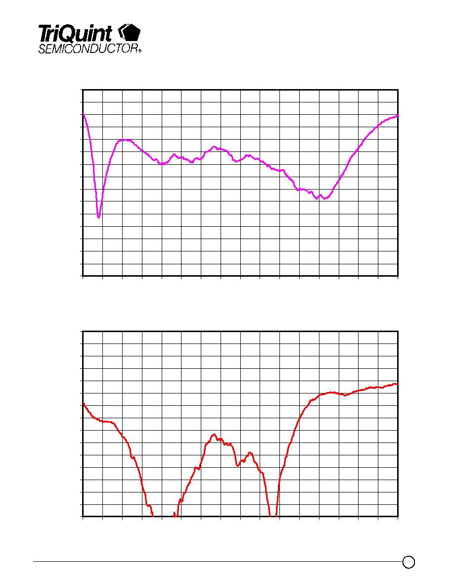
Measured Data
Bias Conditions:
Self Bias
, Vd = 5 V, Id = 90 mA
0
2
4
6
8
10
12
14
16
18
20
22
24
26
28
30
2
3
4
5
6
7
8
9
10
11
12
13
14
15
16
17
18
Frequency (GHz)
G
a
in
(
d
B
)
0
2
4
6
8
10
12
14
16
18
20
22
24
26
28
30
2
3
4
5
6
7
8
9
10
11
12
13
14
15
16
17
18
Frequency (GHz)
Ga
i
n
Ov
e
r
V
c
trl (d
B
)
Vctrl=0.0V
Vctrl=2.5V
Vctrl=2.75V
Vctrl=3.0V
Vctrl=3.25V
Vctrl=3.5V
Vctrl=3.75V
Vctrl=4.0V
Vctrl=4.25V
Vctrl=4.5V
Vctrl=5.0V

TriQuint Semiconductor Texas: Phone (972)994-8465 Fax (972)994-8504 Email: Info-mmw@tqs.com Web: www.triquint.com
Advance Product Information
July 15, 2005
5
TGA2512-SM
Measured Data
Bias Conditions:
Self Bias
, Vd = 5 V, Id = 90 mA
-30
-28
-26
-24
-22
-20
-18
-16
-14
-12
-10
-8
-6
-4
-2
0
2
3
4
5
6
7
8
9
10
11
12
13
14
15
16
17
18
Frequency (GHz)
I
npu
t
Ret
ur
n
L
oss
(
dB)
-30
-28
-26
-24
-22
-20
-18
-16
-14
-12
-10
-8
-6
-4
-2
0
2
3
4
5
6
7
8
9
10
11
12
13
14
15
16
17
18
Frequency (GHz)
Out
put
R
e
t
u
r
n
Los
s (
dB)
