Advance Product Information
November 9, 2004
1
TriQuint Semiconductor Texas Phone: (972)994-8465 Fax: (972)994 8504 Email: info-mmw@tqs.com Web: www.triquint.com
Ku Band 6.5 W Power Amplifier TGA2514-EPU
Primary Applications
∑
Ku band VSAT Transmitter
∑
Point to Point Radio
Key Features
∑
Frequency Range: 13 - 18 GHz
∑
38.5 dBm Nominal Psat from 13.75 - 14 GHz
∑
38 dBm Nominal Psat from 13-16 GHz
∑
37.5 dBm Nominal Psat from 16-18 GHz
∑
33 dBc IMD3 @ 27 dBm Pout/tone @ 14 GHz
∑
24 dB Nominal Gain
∑
12 dB Nominal Return Loss
∑
0.25-µm 3MI pHEMT Technology
∑
Bias Conditions: 8 V @ 2.6 A Idq
∑
Chip size: 2.87 x 3.90 x .10 mm
∑
(0.113 x 0.154 x 0.004)
Measured Fixtured Data
Bias Conditions: Vd = 8 V, Idq = 2.6A
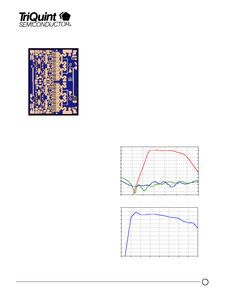
Product Description
The TriQuint TGA2514-EPU is a compact
6.5 W Ku-band Power Amplifier which
operates from 13-18 GHz. The
TGA2514-EPU is designed using
TriQuint's proven standard 0.25-µm gate
pHEMT production process.
The TGA2514-EPU provides a nominal
38 dBm of saturated power with a small
signal gain of 24 dB. Typical return loss
is 14 dB.
The TGA2514-EPU is 100% DC and RF
tested on-wafer to ensure performance
compliance.
-28
-24
-20
-16
-12
-8
-4
0
4
8
12
16
20
24
28
8
10
12
14
16
18
20
22
Frequency (GHz)
Gain
(d
B)
-28
-24
-20
-16
-12
-8
-4
0
4
8
12
16
20
24
28
Retu
r
n
L
o
ss (d
B)
28
29
30
31
32
33
34
35
36
37
38
39
40
12
13
14
15
16
17
18
19
20
Frequency (GHz)
Psat (d
Bm)
Note: This device is early in the characterization process prior to finalizing all electrical specifications. Specifications are subject to
change without notice.

Advance Product Information
November 9, 2004
2
TriQuint Semiconductor Texas Phone: (972)994-8465 Fax: (972)994 8504 Email: info-mmw@tqs.com Web: www.triquint.com
TABLE I
MAXIMUM RATINGS
Symbol
Parameter 1/
Value
Notes
V
+
Positive Supply Voltage
9 V
2/
V
-
Negative Supply Voltage Range
-5V TO 0V
I
+
Positive Supply Current
4 A
2/
| I
G
|
Gate Supply Current
113 mA
P
IN
Input Continuous Wave Power
30.3 dBm
2/
P
D
Power Dissipation
20.8 W
2/, 3/
T
CH
Operating Channel Temperature
150
0
C
4/, 5/
T
M
Mounting Temperature
(30 Seconds)
320
0
C
T
STG
Storage Temperature
-65 to 150
0
C
1/
These ratings represent the maximum operable values for this device.
2/
Combinations of supply voltage, supply current, input power, and output power shall not
exceed P
D
.
3/
When operated at this bias condition with a base plate temperature of 70
0
C,
the median life is 1E+6 hours.
4/ Junction operating temperature will directly affect the device median time to failure (T
M
).
For maximum life, it is recommended that junction temperatures be maintained at the
lowest possible levels.
5/
These ratings apply to each individual FET.
TGA2514-EPU
Advance Product Information
November 9, 2004
3
TriQuint Semiconductor Texas Phone: (972)994-8465 Fax: (972)994 8504 Email: info-mmw@tqs.com Web: www.triquint.com
TABLE III
THERMAL INFORMATION
Parameter
Test Conditions
T
CH
(
o
C)
R
T
JC
(
q
C/W)
T
M
(HRS)
R
JC
Thermal
Resistance
(channel to backside of
carrier)
Vd = 8 V
I
D
= 2.6 A
Pdiss = 20.8 W
150
3.9
1 E+6
Note: Assumes eutectic attach using 1.5 mil 80/20 AuSn mounted to a 20 mil
CuMo Carrier at 70
∞
C baseplate temperature. Worst case condition with no RF
applied, 100% of DC power is dissipated.
TABLE II
RF CHARACTERIZATION TABLE
(T
A
= 25
q
C, Nominal)
(Vd = 8V, Id = 2.6 A)
SYMBOL
PARAMETER
TEST
CONDITION
TYPICAL
UNITS
Gain
Small Signal Gain
f = 13-18 GHz
24
dB
IRL
Input Return Loss
f = 13-18 GHz
12
dB
ORL
Output Return Loss
f = 13-18 GHz
12
dB
Psat
Saturated Power
f = 13-16 GHz
f = 16-18 GHz
38
37.5
dBm
TOI
Third Order Intercept
@ Pout/tone = 27dBm
f = 14 GHz
44
dBm
IMD3
Output IMD3 @
Pout/tone = 27 dBm
f = 14 GHz
33
dBc
Note: Table III Lists the RF Characteristics of typical devices as determined by
fixtured measurements.
TGA2514-EPU

Advance Product Information
November 9, 2004
4
TriQuint Semiconductor Texas Phone: (972)994-8465 Fax: (972)994 8504 Email: info-mmw@tqs.com Web: www.triquint.com
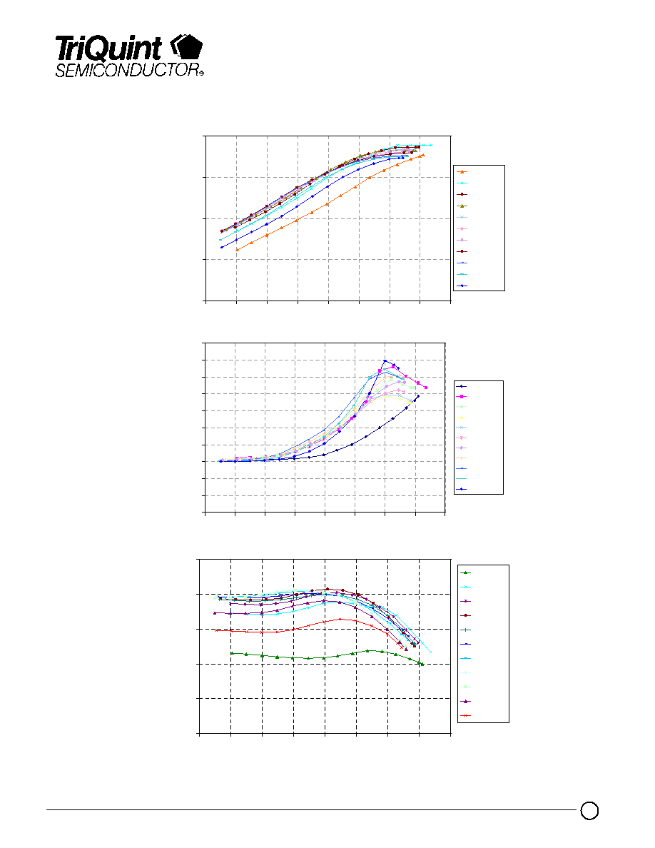
Bias Conditions: Vd = 8 V, Idq = 2.6A
Measured Fixture Data
-28
-24
-20
-16
-12
-8
-4
0
4
8
12
16
20
24
28
8
10
12
14
16
18
20
22
Frequency (GHz)
Gain (dB)
-28
-24
-20
-16
-12
-8
-4
0
4
8
12
16
20
24
28
Return Loss (dB)
28
29
30
31
32
33
34
35
36
37
38
39
40
12
13
14
15
16
17
18
19
20
Frequency (GHz)
Output Power (dBm)
Psat
P1dB
TGA2514-EPU
Advance Product Information
November 9, 2004
5
TriQuint Semiconductor Texas Phone: (972)994-8465 Fax: (972)994 8504 Email: info-mmw@tqs.com Web: www.triquint.com
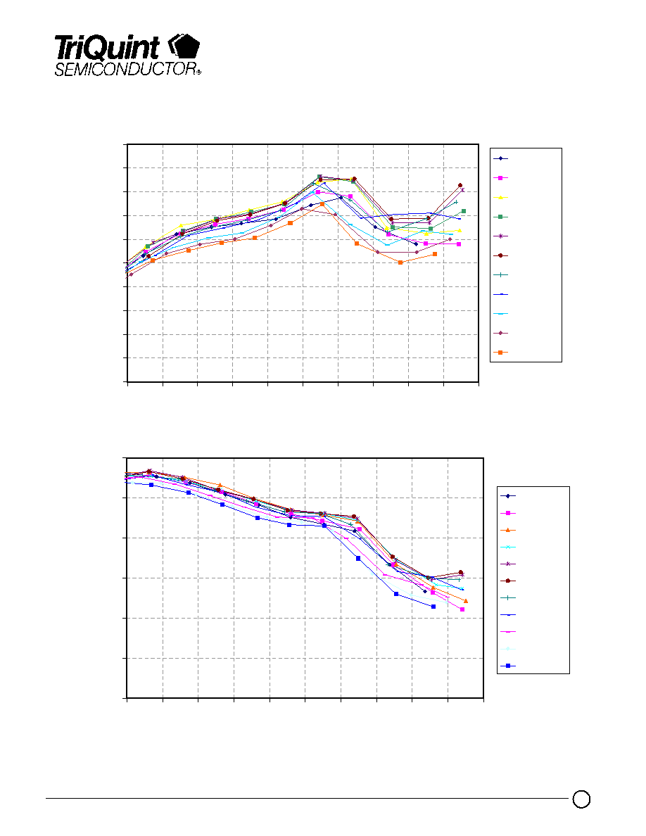
Bias Conditions: Vd = 8 V, Idq = 2.6A
Measured Fixture Data
2
2.2
2.4
2.6
2.8
3
3.2
3.4
3.6
3.8
4
4
6
8
10
12
14
16
18
20
Pin (dBm)
Drai
n Current (A)
13GHz
13.5 GHz
14 GHz
14.5 GHz
15GHz
15.5GHz
16 GHz
16.5GHz
17 Ghz
17.5 GHz
18 GHz
16
18
20
22
24
26
4
6
8
10
12
14
16
18
20
Pin (dBm)
Po
wer
Gai
n
(d
B
)
13GHz
13.5 GHz
14 GHz
14.5 GHz
15GHz
15.5GHz
16 GHz
16.5GHz
17 Ghz
17.5 GHz
18 GHz
20
25
30
35
40
4
6
8
10
12
14
16
18
20
Pin (dBm)
Pout(dBm)
13 GHz
13.5 GHz
14 GHz
14.5 GHz
15 GHz
15.5 GHz
16 GHz
16.5 GHz
17 GHz
17.5 GHz
18 GHz
TGA2514-EPU
Advance Product Information
November 9, 2004
6
TriQuint Semiconductor Texas Phone: (972)994-8465 Fax: (972)994 8504 Email: info-mmw@tqs.com Web: www.triquint.com
Bias Conditions: Vd = 8 V, Idq = 2.6A
Measured Fixture Data
0
10
20
30
40
50
60
12
14
16
18
20
22
24
26
28
30
32
Output Power/Tone (dBm)
IMD3 (dBc)
13 GHz
13.5 GHz
14 GHz
14.5GHz
15 GHz
15.5 GHz
16 GHz
16.5 GHz
17 GHz
17.5 GHz
18 GHz
30
32
34
36
38
40
42
44
46
48
50
12
14
16
18
20
22
24
26
28
30
32
Output Power/Tone (dBm)
TOI (dBm)
13 GHz
13.5 GHz
14 GHz
14.5GHz
15 GHz
15.5 GHz
16 GHz
16.5 GHz
17 GHz
17.5 GHz
18 GHz
TGA2514-EPU
Advance Product Information
November 9, 2004
7
TriQuint Semiconductor Texas Phone: (972)994-8465 Fax: (972)994 8504 Email: info-mmw@tqs.com Web: www.triquint.com
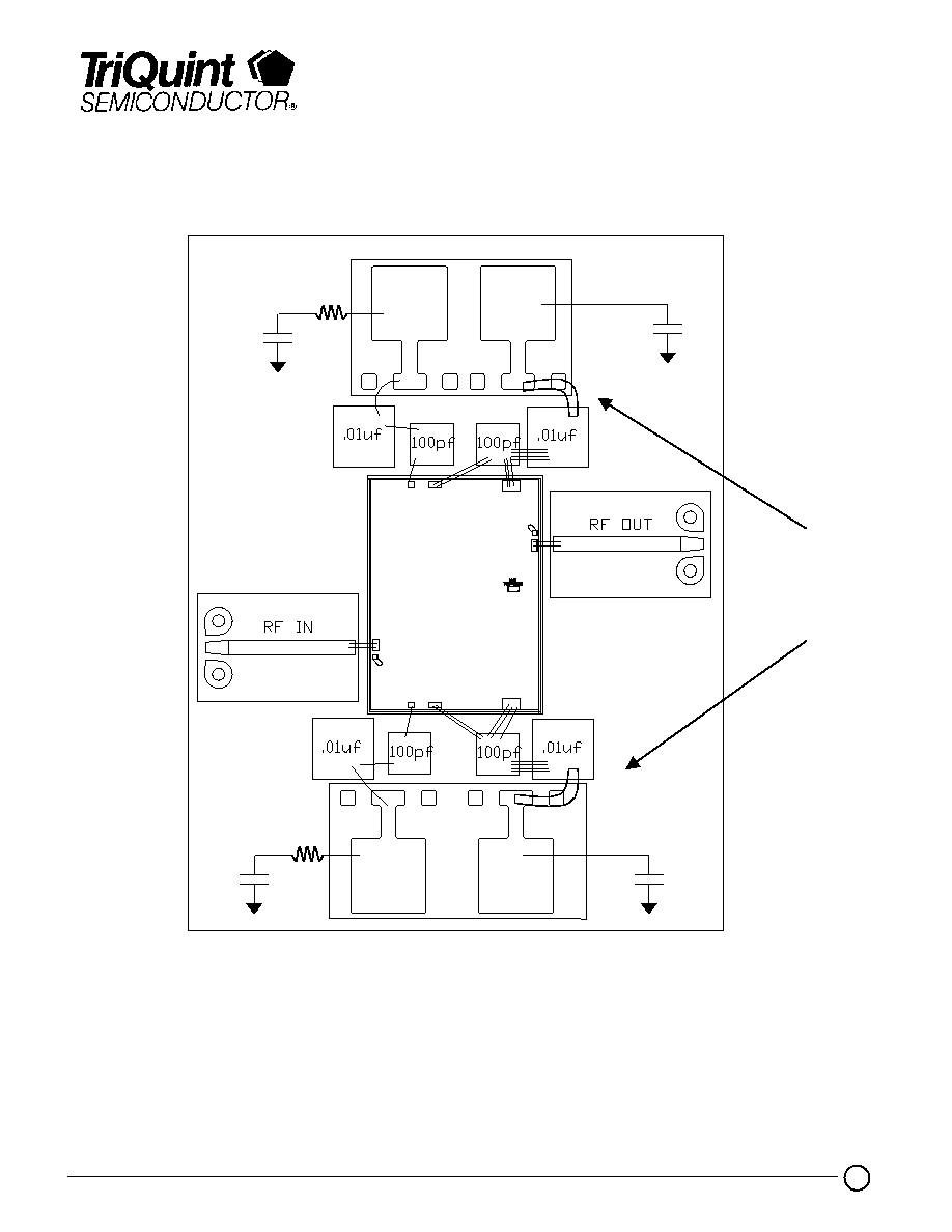
Vg
Vg
Vd
Vd
Recommended Chip Assembly Diagram
GaAs MMIC devices are susceptible to damage from Electrostatic Discharge. Proper precautions should
be observed during handling, assembly and test.
20 mil ribbon
Notes:
1. Vg can be connected from either side, but 100 pf, 0.01 uf , 1uf caps and 10 ohm resistor are
needed for both sides.
2. Vd connection must be biased from both sides.
10
:
1
P
F
10
:
1
P
F
1
P
F
1
P
F
TGA2514-EPU
Advance Product Information
November 9, 2004
8
TriQuint Semiconductor Texas Phone: (972)994-8465 Fax: (972)994 8504 Email: info-mmw@tqs.com Web: www.triquint.com
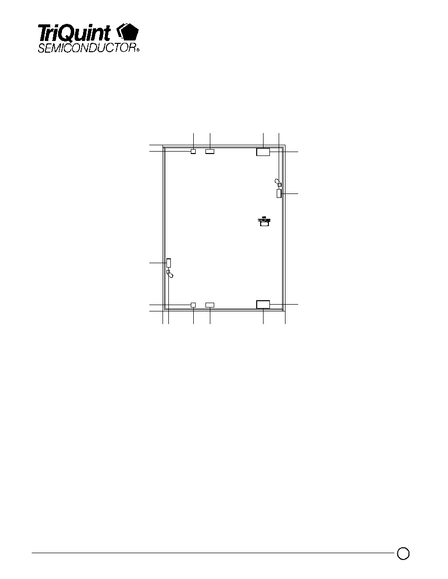
Mechanical Drawing
GaAs MMIC devices are susceptible to damage from Electrostatic Discharge. Proper precautions should
be observed during handling, assembly and test.
0.000 (0.000)
0.148 (0.006)
1.136 (0.045)
3.748 (0.148)
3.903 (0.154)
0.161 (0.006)
2.764 (0.109)
3.742 (0.147)
0.
00
0 (
0
.0
00
)
0.
14
2 (
0
.0
06
)
0.
72
2 (
0
.0
28
)
1.11
3 (0
.044
)
2
.
35
8 (
0
.0
93
)
2
.
87
2 (
0
.1
13
)
0.72
2 (
0
.028
)
1.
11
3 (
0
.0
44
)
2.3
58 (0
.09
3
)
2.7
32 (0
.10
8
)
1
2
3
4
5
6
7
8
Units: Millimeters (inches)
Thickness: 0.100 (0.004) (reference only)
Chip edge to bond pad dimensions are shown to center of bond pad
Chip size +/- 0.05 (0.002)
GND IS BACKSIDE OF MMIC
RF Input
Vg
Vd
Vd
RF Output
Bond pad #1
Bond pads #2, 8
Bond pads #3, 7
Bond pads # 4, 6
Bond pad #5
0.096 x 0.200 (0.004 x 0.008)
0.098 x 0.098 (0.004 x 0.004)
0.198 x 0.100 (0.008 x 0.004)
0.296 x 0.178 (0.012 x 0.007)
0.096 x 0.200 (0.004 x 0.008)
TGA2514-EPU

Advance Product Information
November 9, 2004
9
TriQuint Semiconductor Texas Phone: (972)994-8465 Fax: (972)994 8504 Email: info-mmw@tqs.com Web: www.triquint.com
Assembly Process Notes
GaAs MMIC devices are susceptible to damage from Electrostatic Discharge. Proper precautions should
be observed during handling, assembly and test.
Reflow process assembly notes:
∑
Use AuSn (80/20) solder with limited exposure to temperatures at or above 300
∞
C
(for 30 sec max).
∑
An alloy station or conveyor furnace with reducing atmosphere should be used.
∑
No fluxes should be utilized.
∑
Coefficient of thermal expansion matching is critical for long-term reliability.
∑
Devices must be stored in a dry nitrogen atmosphere.
Component placement and adhesive attachment assembly notes:
∑
Vacuum pencils and/or vacuum collets are the preferred method of pick up.
∑
Air bridges must be avoided during placement.
∑
The force impact is critical during auto placement.
∑
Organic attachment can be used in low-power applications.
∑
Curing should be done in a convection oven; proper exhaust is a safety concern.
∑
Microwave or radiant curing should not be used because of differential heating.
∑
Coefficient of thermal expansion matching is critical.
Interconnect process assembly notes:
∑
Thermosonic ball bonding is the preferred interconnect technique.
∑
Force, time, and ultrasonics are critical parameters.
∑
Aluminum wire should not be used.
∑
Discrete FET devices with small pad sizes should be bonded with 0.0007-inch wire.
∑
Maximum stage temperature is 200
∞
C.
TGA2514-EPU