TriQuint Semiconductor Texas: Phone (972)994-8465 Fax (972)994-8504 Email: Info-mmw@tqs.com Web: www.triquint.com
Advance Product Information
April 27, 2005
1
25
26
27
28
29
30
31
32
33
34
35
3.1
3.2
3.3
3.4
3.5
3.6
3.7
3.8
3.9
Frequency (GHz)
Out
put
P
o
wer (
d
Bm
)
-20
-15
-10
-5
0
5
10
15
20
25
30
3.3
3.4
3.5
3.6
3.7
3.8
Frequency (GHz)
S-
Param
e
t
e
r (
d
B
)
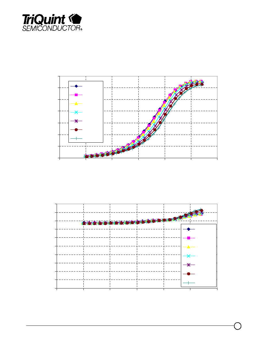
3.5GHz WiMAX Driver / Power Amplifier TGA2703-SM
Key Features
∑ 3.3-3.8 GHz Bandwidth
∑ 41 dBc IMR3 @ 21 dBm Pout/tone
∑ 24 dB Nominal Gain
∑ 30 dBm Nominal P1dB
∑ 2.5% EVM at 22 dBm output power
∑ 13 dB step attenuator function
∑ Power sample port
∑ -1.5V Vg voltage to shut down drain current
∑ Self bias: +6 V 770mA
∑ Package Dimensions:
5.0 x 5.0 x 0.9 mm QFN
Primary Applications
∑ Fixed Broadband Wireless
∑ WiMAX
Preliminary Measured Data
Bias Conditions: Vd = +6 V Self Bias
P2dB
P1dB
S21
S11
S22
General Description
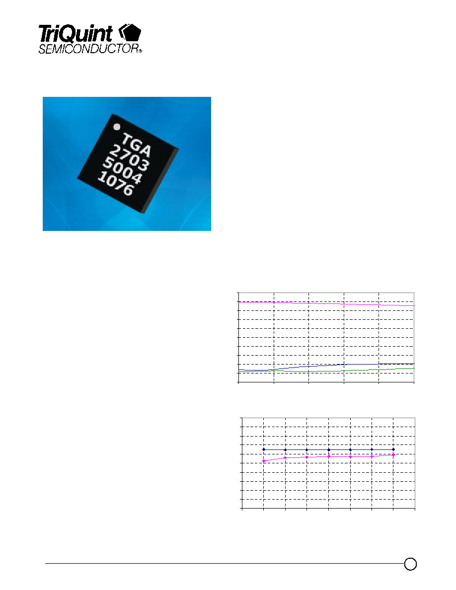
TGA2703-SM is a linear amplifier
operating for 802.16 broadband
wireless applications in 3.3 to 3.8 GHz
frequency band. The PA delivers 24 dB
of small-signal gain, 30dBm P1dB and
40 dBc IMR3 at 21 dBm output power
per tone from a single +6V power
supply. It has 2.5% EVM at 22 dBm
output power. The TGA2703
incorporates a 13 dB step attenuator
function and a power sampling port.
The 50 ohm device requires minimum
external components for operation, and
is packaged in a low-cost, surface
mount 5x5 QFN style package.
Lead-Free & RoHS compliant.
Demo boards are available.
Note: This device is early in the characterization process prior to finalizing all electrical specifications. Specifications are subject to
change without notice.

TriQuint Semiconductor Texas: Phone (972)994-8465 Fax (972)994-8504 Email: Info-mmw@tqs.com Web: www.triquint.com
Advance Product Information
April 27, 2005
2
TGA2703-SM
TABLE I
MAXIMUM RATINGS 1/
SYMBOL
PARAMETER
VALUE
NOTES
Vd
Drain Voltage
7 V
2/
Vctrl
Gain Control Voltage
7 V
Id
Drain Current
1.1 A
2/ 3/
Ig
Gate Current
6 mA
3/
P
IN
Input Continuous Wave Power
25 dBm
P
D
Power Dissipation
4.68W
2/ 4/
T
CH
Operating Channel Temperature
150
0
C
5/
T
M
Mounting Temperature (30 Seconds)
260
0
C
T
STG
Storage Temperature
-65 to 150
0
C
1/
These ratings represent the maximum operable values for this device.
2/
Combinations of supply voltage, supply current, input power, and output power shall not exceed P
D
.
3/
Total current for the device.
4/
When operated at this bias condition with a base plate temperature of 85
0
C, the median life is
reduced.
5/
Junction operating temperature will directly affect the device median time to failure (MTTF). For
maximum life, it is recommended that junction temperatures be maintained at the lowest possible
levels.

TriQuint Semiconductor Texas: Phone (972)994-8465 Fax (972)994-8504 Email: Info-mmw@tqs.com Web: www.triquint.com
Advance Product Information
April 27, 2005
3
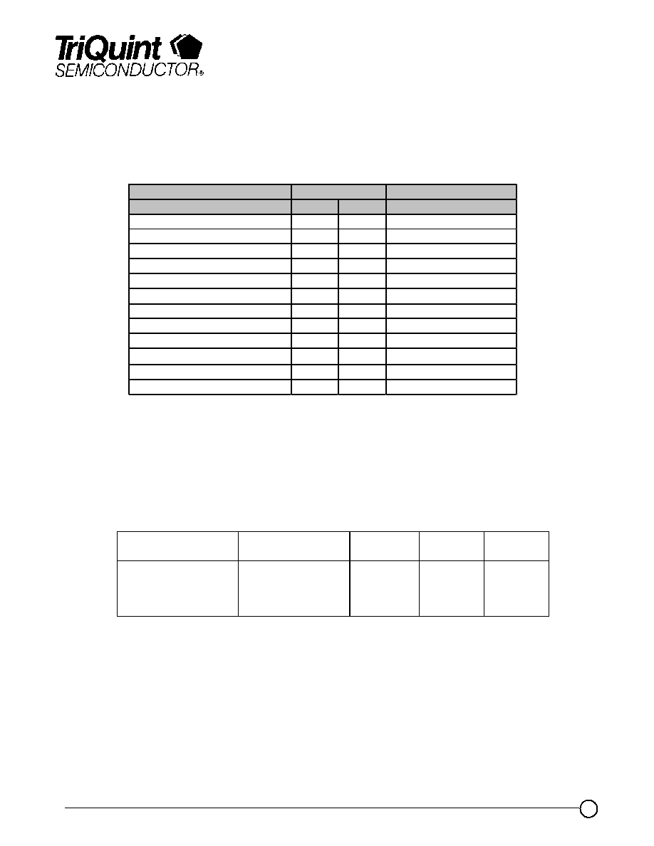
TABLE II
ELECTRICAL CHARACTERISTICS
(Ta = 25
0
C Nominal)
Notes
Response
Units
Typical
Frequency Band
GHz
3.3-3.8GHz
Drain Operating Voltage
V
6
Small Signal Gain
dB
24
Input Return Loss
dB
10
Output Return Loss
dB
12
Control Gain Step
dB
13
Psat
dBm
31.5
Pin at 11 dBm
P1dB
dBm
30
EVM
%
TBD
at 3.5 GHz, 23 dBm Pout
Gain variation over temperature
dB/
o
C
0.03
IMD3
dBc
41
at 21 dBm Pout/tone
TOI
dBm
42
at 21 dBm Pout/tone
TABLE III
THERMAL INFORMATION
Parameter
Test Conditions
T
CH
(
o
C)
R
T
JC
(
q
C/W)
T
M
(HRS)
R
JC
Thermal
Resistance
(channel to backside
of package)
Vd = 6V
I
D
= 0.77 A
Pdiss = 4.62 W
145.5
13.1
3.8E+6
Note: Package backside soldered to carrier at 85
∞
C baseplate temperature.
TGA2703-SM

TriQuint Semiconductor Texas: Phone (972)994-8465 Fax (972)994-8504 Email: Info-mmw@tqs.com Web: www.triquint.com
Advance Product Information
April 27, 2005
4
25
26
27
28
29
30
31
32
33
34
35
3.1
3.2
3.3
3.4
3.5
3.6
3.7
3.8
3.9
Frequency (GHz)
O
u
t
put
Pow
e
r (
d
Bm)
-30
-20
-10
0
10
20
30
2
2.5
3
3.5
4
4.5
5
Frequency (GHz)
S Parameter (dB)
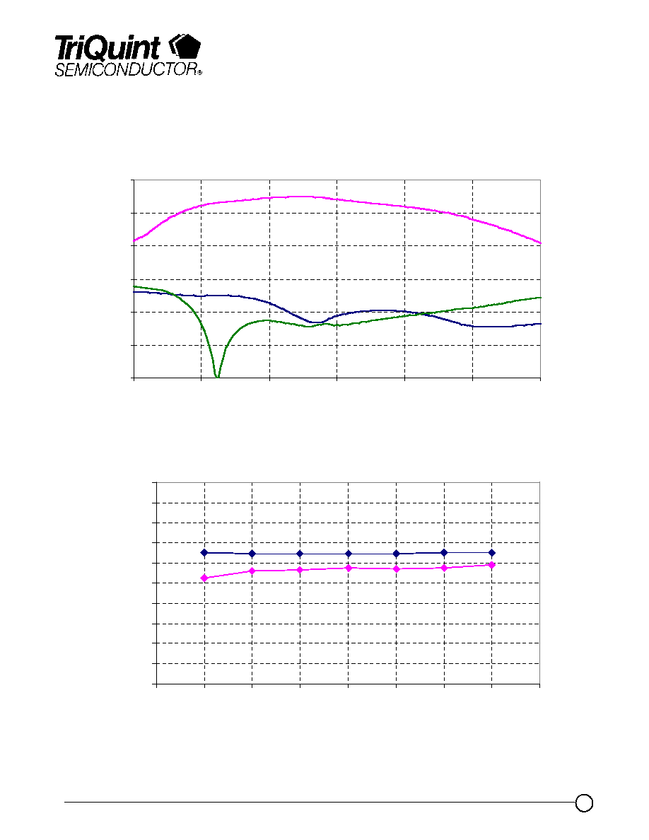
Measured Data
Bias Conditions: Vd = 6 V, Id =770 mA Self Bias
S21
S11
S22
P2dB
P1dB
TGA2703-SM

TriQuint Semiconductor Texas: Phone (972)994-8465 Fax (972)994-8504 Email: Info-mmw@tqs.com Web: www.triquint.com
Advance Product Information
April 27, 2005
5
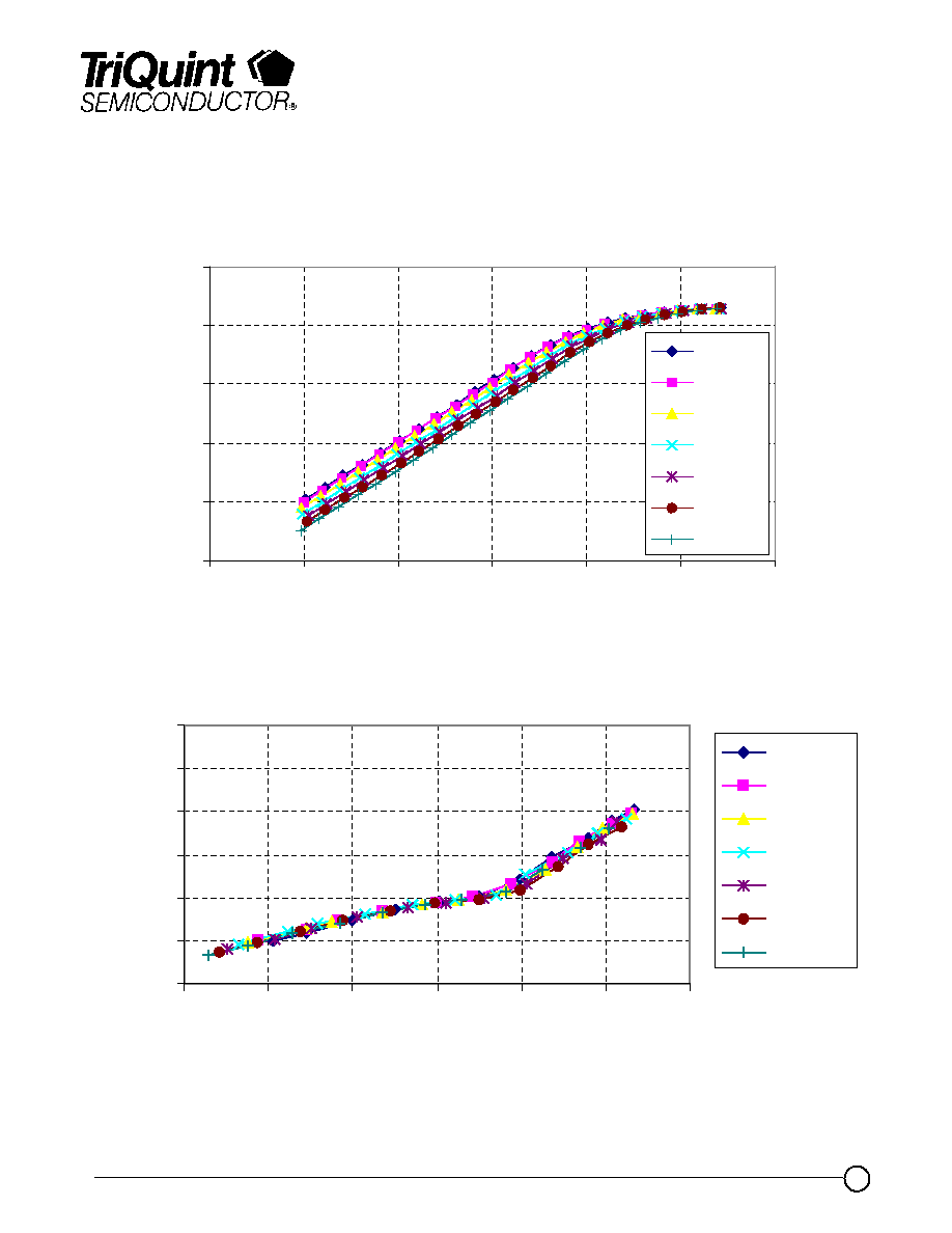
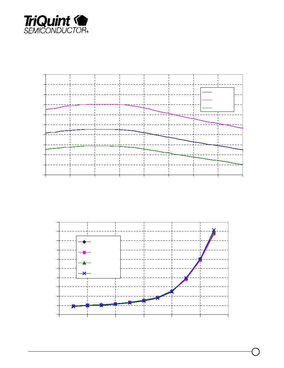
Measured Data
Bias Conditions: Vd = 6 V, Id =770 mA Self Bias
TGA2703-SM
10
15
20
25
30
35
-15
-10
-5
0
5
10
15
Pin (dBm)
Pout (dBm)
3.2GHz
3.3GHz
3.4GHz
3.5GHz
3.6GHz
3.7GHz
3.8GHz
-60
-50
-40
-30
-20
-10
0
15
17
19
21
23
25
27
Output Power per Tone (dBm)
IMR3
(d
Bc
)
3.35GHz
3.4GHz
3.45GHz
3.5GHz
3.55GHz
3.6GHz
3.65GHz

TriQuint Semiconductor Texas: Phone (972)994-8465 Fax (972)994-8504 Email: Info-mmw@tqs.com Web: www.triquint.com
Advance Product Information
April 27, 2005
6
Measured Data
Bias Conditions: Vd = 6 V, Id =770 mA Self Bias
TGA2703-SM
0
0.1
0.2
0.3
0.4
0.5
0.6
0.7
0.8
0.9
1
-15
-10
-5
0
5
10
15
Pin (dBm)
Id (A
)
3.2GHz
3.3GHZ
3.4GHz
3.5GHz
3.6GHz
3.7GHz
3.8GHz
0
4
8
12
16
20
24
28
-15
-10
-5
0
5
10
15
Pin (dBm)
PA
E (%
)
3.2GHz
3.3GHz
3.4GHz
3.5GHz
3.6GHz
3.7GHz
3.8GHz

TriQuint Semiconductor Texas: Phone (972)994-8465 Fax (972)994-8504 Email: Info-mmw@tqs.com Web: www.triquint.com
Advance Product Information
April 27, 2005
7
Measured Data
Bias Conditions: Vd = 6 V, Id =770 mA Self Bias
TGA2703-SM
20
21
22
23
24
25
26
27
28
29
30
3
3.1
3.2
3.3
3.4
3.5
3.6
3.7
3.8
Frequency (GHz)
S21 (
d
B)
25 degC
-40 degC
70 degC
OFDM 64 QAM
0
1
2
3
4
5
6
7
8
9
10
14
16
18
20
22
24
26
Output Power (dBm)
EVM (%)
3.35GHz
3.45GHz
3.55GHz
3.65GHz

TriQuint Semiconductor Texas: Phone (972)994-8465 Fax (972)994-8504 Email: Info-mmw@tqs.com Web: www.triquint.com
Advance Product Information
April 27, 2005
8
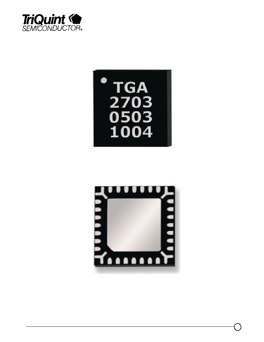
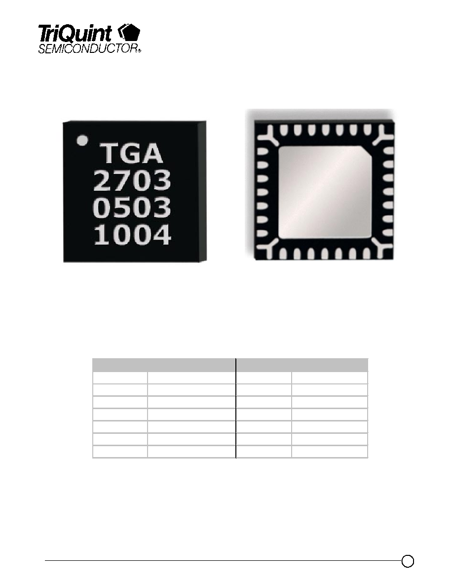
Package Layout
Top View
Bottom View
TGA2703-SM

TriQuint Semiconductor Texas: Phone (972)994-8465 Fax (972)994-8504 Email: Info-mmw@tqs.com Web: www.triquint.com
Advance Product Information
April 27, 2005
9
Package Pinout Diagram
Top Side
Dot indicates Pin 1
Bottom Side
Pin
Description
Pin
Description
1,2,3
NC
14
Power
Sample
4
RF Input
18
RF Output
5,6,7,8,9
NC
19,20,21
NC
10
Gain Control
22
Vd2
11,13
NC
23,24,25
NC
12
Gate Acess
26
Vd1
15,16,17
NC
27,28
NC
1
7
8
14
15
21
22
28
TGA2703-SM
GND

TriQuint Semiconductor Texas: Phone (972)994-8465 Fax (972)994-8504 Email: Info-mmw@tqs.com Web: www.triquint.com
Advance Product Information
April 27, 2005
10
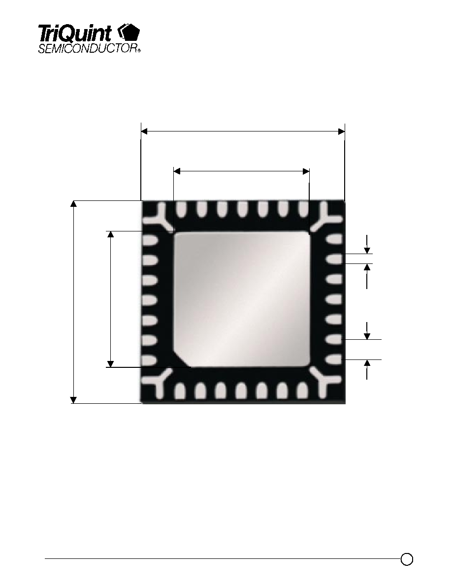
Mechanical Drawing
(Bottom Side)
Units: mm [Inch]
Package tolerance: +/- 0.05
TGA2703-SM
0.31 [0.012]
5.00 [0.197]
3.50 [0.138]
5.00 [0.197]
3.50 [0.138]
0.50 [0.02]

TriQuint Semiconductor Texas: Phone (972)994-8465 Fax (972)994-8504 Email: Info-mmw@tqs.com Web: www.triquint.com
Advance Product Information
April 27, 2005
11
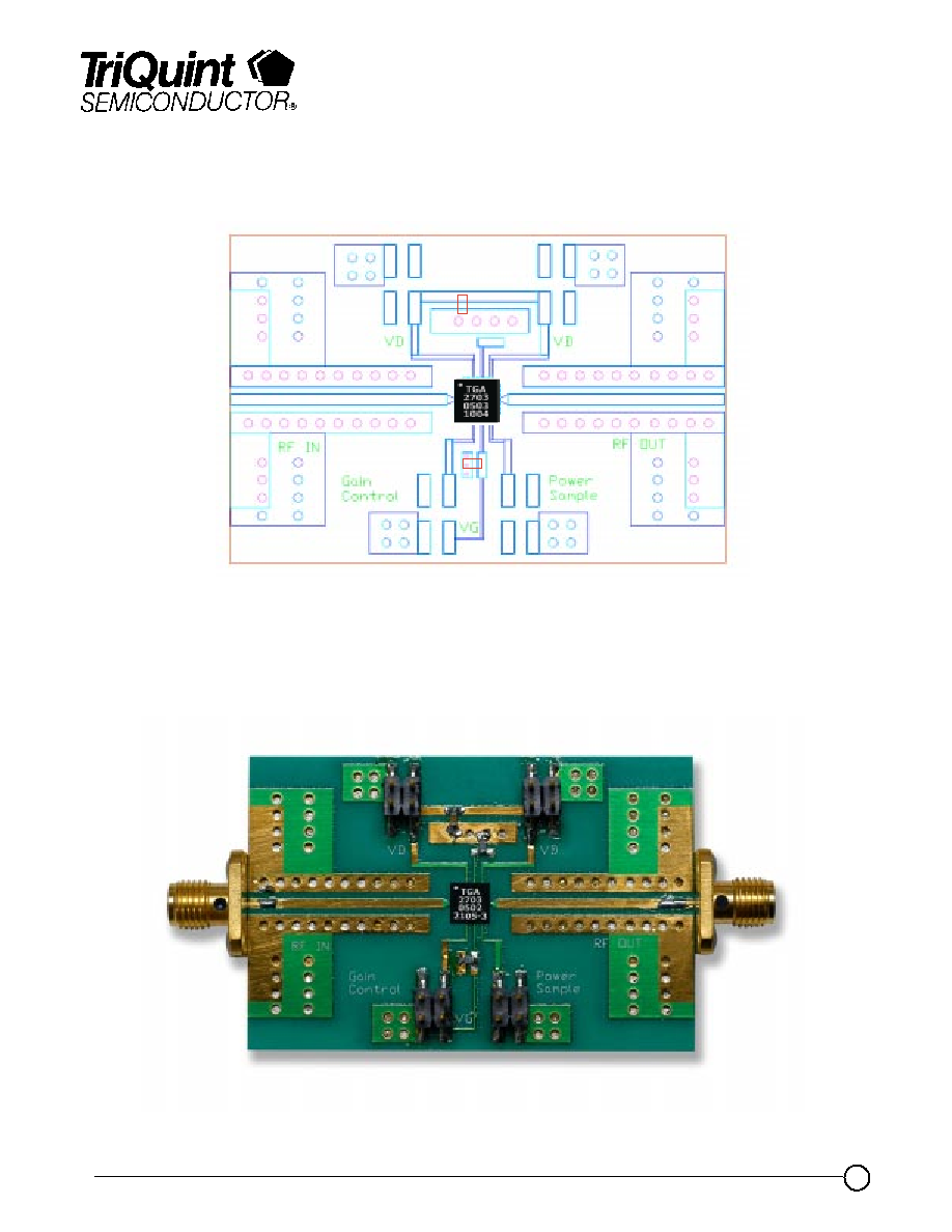
Recommended Board Layout Assembly
∑ The evaluation board material is 20 mil thick RO4003
∑ 100 pF and 0.01 uF are required de-coupling capacitor
TGA2703-SM
0.01uF
100pF

TriQuint Semiconductor Texas: Phone (972)994-8465 Fax (972)994-8504 Email: Info-mmw@tqs.com Web: www.triquint.com
Advance Product Information
April 27, 2005
12
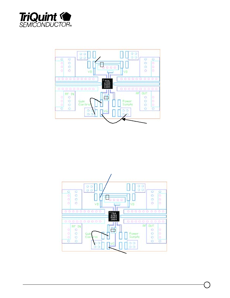
TGA2703 Bias Connection
Self-biased mode
Connect gain control and Vg to ground.
Apply +6V to Vd. Current will be ~770mA
TGA2703-SM
4 inch or longer jumper
Or 10nH inductor
6V
6V
Connect gain control to ground. Apply negative voltage Vg.
Apply +6V to Vd. Current will be ~770mA
Vg
TGA2703 Bias Connection
Gate control mode

TriQuint Semiconductor Texas: Phone (972)994-8465 Fax (972)994-8504 Email: Info-mmw@tqs.com Web: www.triquint.com
Advance Product Information
April 27, 2005
13
TGA2703-SM
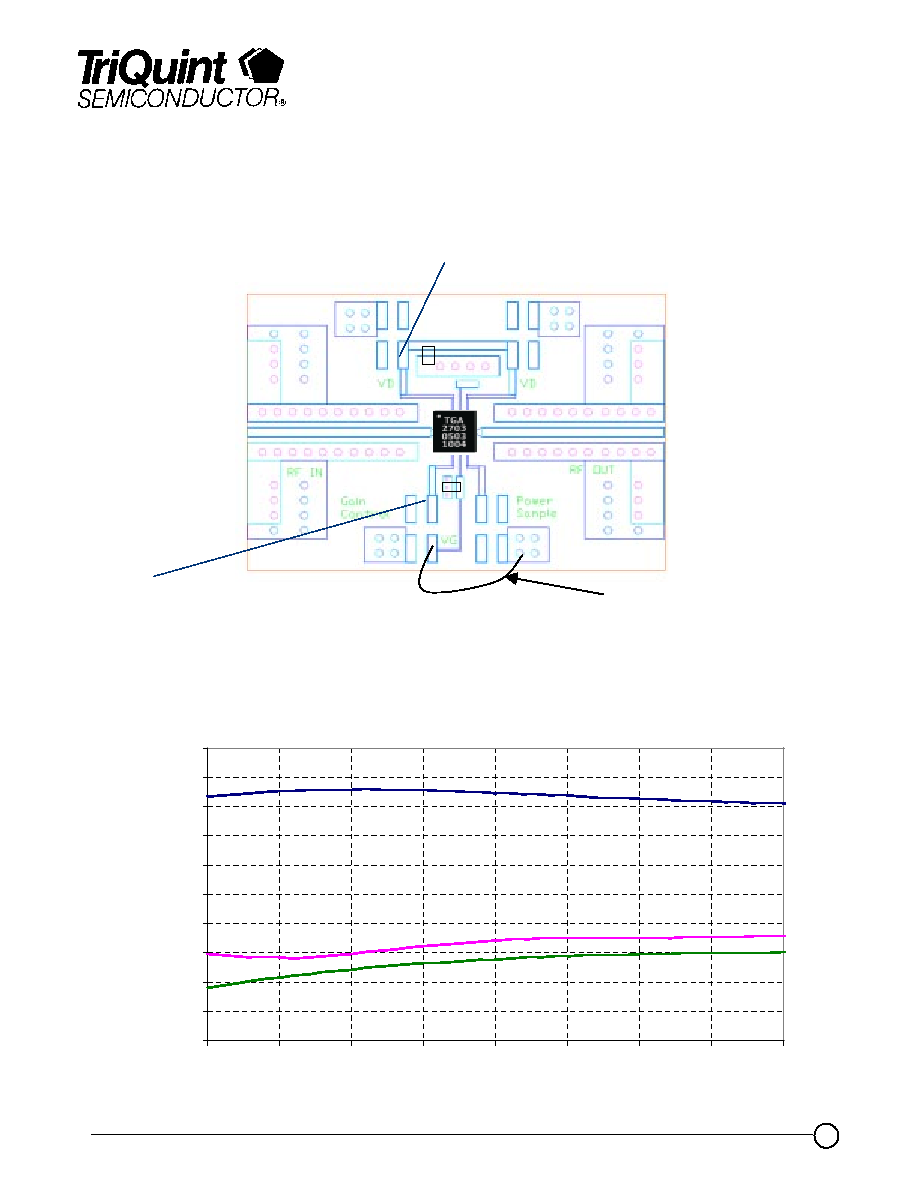
TGA2703 Bias Connection
Gain control mode
6V
6V
For 13 dB attenuation testing:
Connect gain control to +6V and Vg to ground.
Apply +6V to Vd. Current will be ~770mA
4 inch or longer jumper
or 10nH inductor
-30
-25
-20
-15
-10
-5
0
5
10
15
20
3
3.1
3.2
3.3
3.4
3.5
3.6
3.7
3.8
Frequency (GHz)
S-Par
ameter
(d
B
)

TriQuint Semiconductor Texas: Phone (972)994-8465 Fax (972)994-8504 Email: Info-mmw@tqs.com Web: www.triquint.com
Advance Product Information
April 27, 2005
14
TGA2703-SM
Recommended Surface Mount Package Assembly
Proper ESD precautions must be followed while handling packages.
Clean the board with acetone. Rinse with alcohol. Allow the circuit to fully dry.
TriQuint recommends using a conductive solder paste for attachment. Follow solder paste and reflow oven
vendors' recommendations when developing a solder reflow profile. Typical solder reflow profiles are listed
in the table below.
Hand soldering is not recommended. Solder paste can be applied using a stencil printer or dot placement.
The volume of solder paste depends on PCB and component layout and should be well controlled to
ensure consistent mechanical and electrical performance.
Clean the assembly with alcohol.
Typical Solder Reflow Profiles
Reflow Profile
SnPb
Pb Free
Ramp-up Rate
3
∞
C/sec
3
∞
C/sec
Activation Time and
Temperature
60 ≠ 120 sec @ 140 ≠ 160
∞
C
60 ≠ 180 sec @ 150 ≠ 200
∞
C
Time above Melting Point
60 ≠ 150 sec
60 ≠ 150 sec
Max Peak Temperature
240
∞
C
260
∞
C
Time within 5
∞
C of Peak
Temperature
10 ≠ 20 sec
10 ≠ 20 sec
Ramp-down Rate
4 ≠ 6
∞
C/sec
4 ≠ 6
∞
C/sec
