Advance Product Information
July 20, 2005
1
TriQuint Semiconductor Texas: Phone (972)994-8465 Fax (972)994-8504 Email: Info-mmw@tqs.com Web: www.triquint.com
CATV TIA/Gain Block
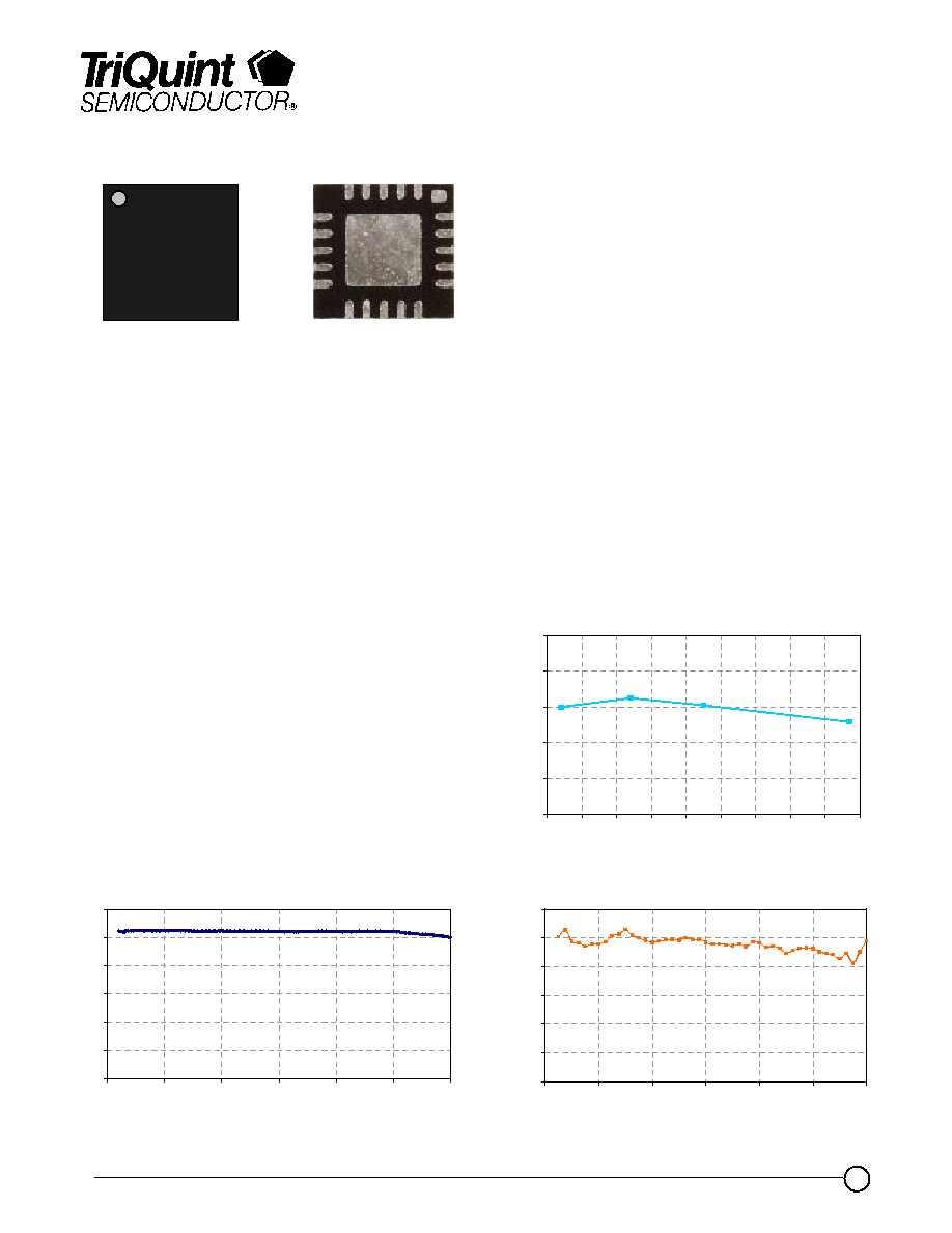
TGA2803-SM
Key Features and Performance
∑
Frequency Range: 40MHz - 1GHz
∑
20 dB Flat Gain
∑
800
Transimpedance *
∑
<5pA/
Hz Equivalent Input Noise Current *
∑
1.5 dB 75
Noise Figure
∑
Ultra-Low Distortion (45dBm IP3 typ.)
∑
Low DC Power Consumption
∑
Single Supply Bias (+8V)
∑
Proven GaAs Technology
∑
20L Package Dimension: 4.0 x 4.0 x 0.9 mm
* Includes 1:1 balun, No photodiode or auto-transformer
Product Description
The TriQuint TGA2803-SM is an ultra-
linear, packaged TIA/Gain Block
which operates from 40MHz to
1000MHz.
The TGA2803-SM typically provides
flat gain along with ultra-low distortion.
It also provides high output power with
low DC power consumption.
This amplifier is ideally suited for use
in CATV distribution systems or other
applications requiring extremely low
noise and distortion.
Demonstration Boards are available.
Lead-free and RoHS compliant.
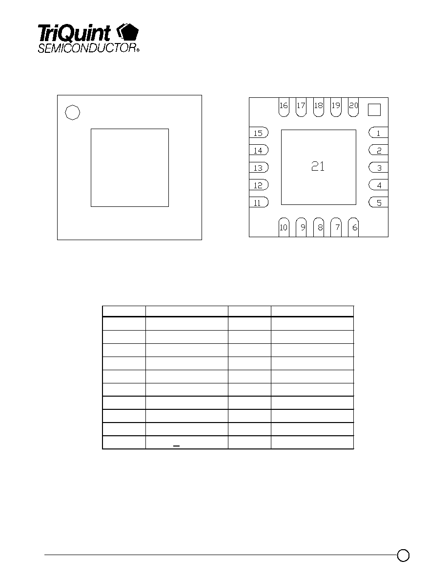
Bottom View
Top View
Primary Applications
∑
HFC Nodes
∑
CATV Line Amplifiers
∑
Head End Equipment
0
4
8
12
16
20
24
0
200
400
600
800
1000
1200
Frequency (MHz)
G
a
in
(d
B
)
Typical 75
:
Gain
w/External Balun Losses Removed
75
:
Output TOI
35
39
43
47
51
55
0
100
200
300
400
500
600
700
800
900
Frequency (MHz)
OTOI (dBm)
Input Referred Current Noise
with High Impedance source
0
1
2
3
4
5
6
0
2 00
4 00
6 00
8 00
10 00
12 00
F re q u e n c y (M H z )
Noi
se Cur
r
ent
(
p
A/
r
t
(
H
z)
)
TGA
2803
Note: This device is early in the characterization process prior to finalizing all electrical specifications. Specifications are subject to
change without notice.

Advance Product Information
July 20, 2005
2
TriQuint Semiconductor Texas: Phone (972)994-8465 Fax (972)994-8504 Email: Info-mmw@tqs.com Web: www.triquint.com
TGA2803-SM
Table II
DC Specifications
Symbol
Parameter
Typ
Unit
V
DD
Bias Supply Voltage
8
V
I
DD
Bias Supply Current
350
mA
V
G1
Gate 1 Voltage (Pin 19)
0.90
V
V
G2
Gate 2 Voltage (Pin 7)
2.66
V
V
out1
RF Output 1 Voltage (Pin 14/15)
V
DD
V
V
out2
RF Output 2 Voltage (Pin 11/12)
V
DD
V
Table I
Maximum Ratings 1/
Symbol
Parameter
Min
Max
Units
Notes
V
DD
Bias Supply Voltage
0
15
V
I
DD
Bias Supply Current
500
mA
1/ 2/
P
IN
RF Input Power
77
dBmV
3/
T
ASSY
Assembly Temperature (30 seconds max)
300
∞
C
T
STG
Storage Temperature
-65
150
∞
C
T
CASE
Package Operating Temperature (Heat Slug)
-40
110
∞
C
1/
These values reflect maximum operable values for this device. Operating above the
recommended values may directly affect MTTF.
2/
Total Current
3/
Total Input Power

Advance Product Information
July 20, 2005
3
TriQuint Semiconductor Texas: Phone (972)994-8465 Fax (972)994-8504 Email: Info-mmw@tqs.com Web: www.triquint.com
Table III
RF Specifications 1/
T
A
=25
∞
C, V
DD
=8V
Symbol
Parameter
Min
Typ
Max
Units
Note
BW
Bandwidth
40
870
MHz
S
21
Power Gain
20
dB
2/
GF
Gain Flatness
±
0.3
dB
2/
NF
Noise Figure
1.5
dB
2/
TZ
Transimpedance
800
I
n
Equivalent Input Current Noise
5
pA/rtHz
3/
IP
3
Two-Tone, Third-Order Intercept (450 MHz)
46
dBm
IRL
Input Return Loss
16
dB
ORL
Output Return Loss
20
dB
I
D
Drain Current
350
mA
4/
P1dB
Output Power at P1dB (450 MHz)
27
dBm
1/
Using electrical application circuit on pg. 8
2/
1:1 Balun losses have been removed from the measurement
3/
Measured with open-circuited input
4/
Increasing drain current will improve linearity of device
TGA2803-SM

Advance Product Information
July 20, 2005
4
TriQuint Semiconductor Texas: Phone (972)994-8465 Fax (972)994-8504 Email: Info-mmw@tqs.com Web: www.triquint.com
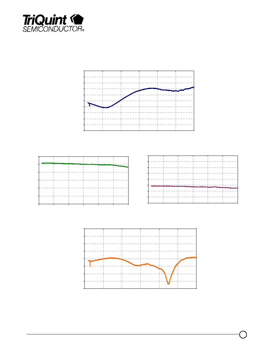
Typical Measured S-Parameters (75
:
)
Using Application Circuit
(includes effects of external baluns)
-40
-36
-32
-28
-24
-20
-16
-12
-8
-4
0
0
200
400
600
800
1000
1200
Frequency (MHz)
S11(
dB
)
0
4
8
12
16
20
24
0
200
400
600
800
1000
1200
Frequency (MHz)
S
21 (
d
B)
-40
-35
-30
-25
-20
-15
-10
-5
0
0
200
400
600
800
1000
1200
Frequency (MHz)
S12 (
d
B)
-40
-35
-30
-25
-20
-15
-10
-5
0
0
200
400
600
800
1000
1200
Frequency (MHz)
S22 (dB
)
TGA2803-SM

Advance Product Information
July 20, 2005
5
TriQuint Semiconductor Texas: Phone (972)994-8465 Fax (972)994-8504 Email: Info-mmw@tqs.com Web: www.triquint.com
0
1
2
3
4
5
6
0
200
400
600
800
1000
1200
Frequency (M H z)
Nois
e
Curre
nt
(
pA/rt
(
H
z)
)
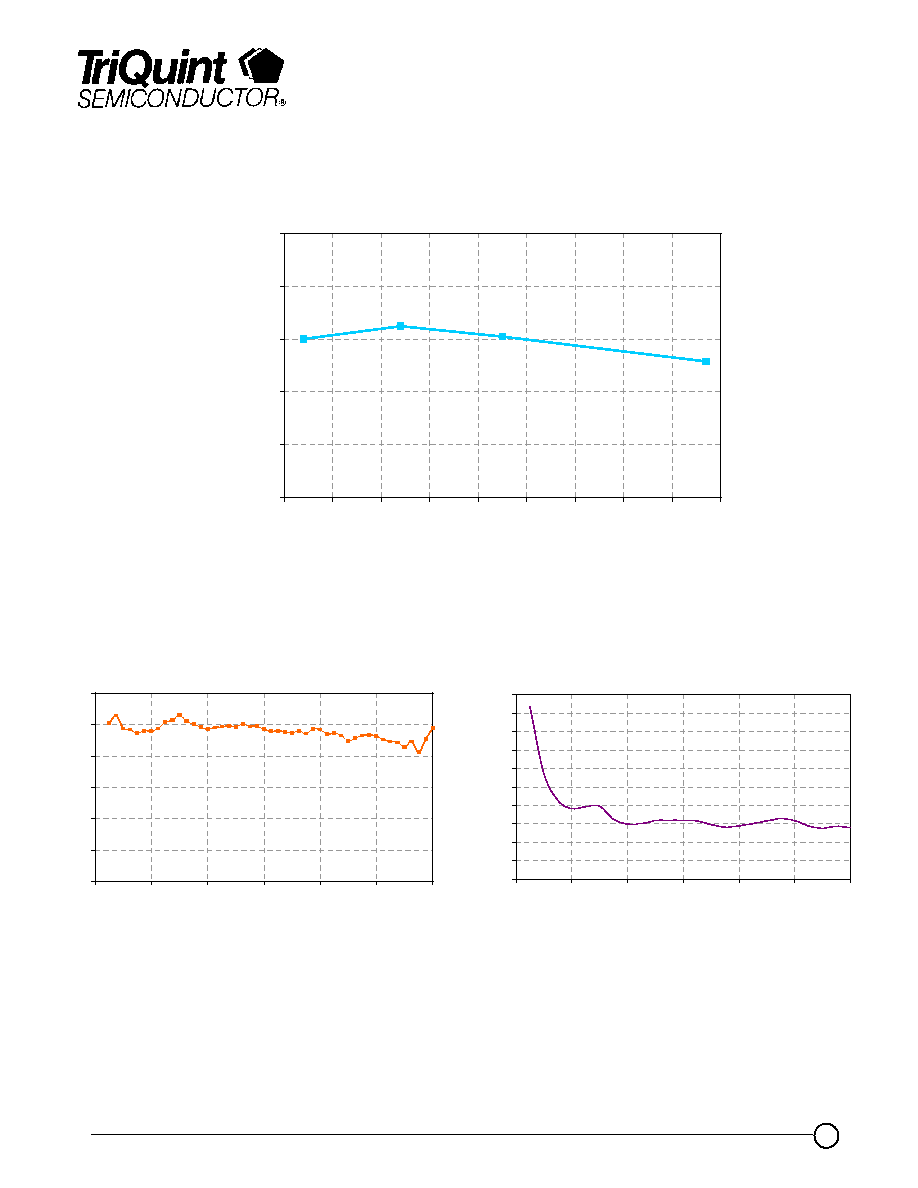
Typical Measured Performance
Using Application Circuit
(includes effects of external baluns)
35
39
43
47
51
55
0
100
200
300
400
500
600
700
800
900
Frequency (MHz)
OTOI (
d
B
m
)
0
0.5
1
1.5
2
2.5
3
3.5
4
4.5
5
0
200
400
600
800
1000
1200
Frequency(MHz)
N
o
i
se F
i
g
u
re(d
B
)
Input balun losses removed
TGA2803-SM

Advance Product Information
July 20, 2005
6
TriQuint Semiconductor Texas: Phone (972)994-8465 Fax (972)994-8504 Email: Info-mmw@tqs.com Web: www.triquint.com
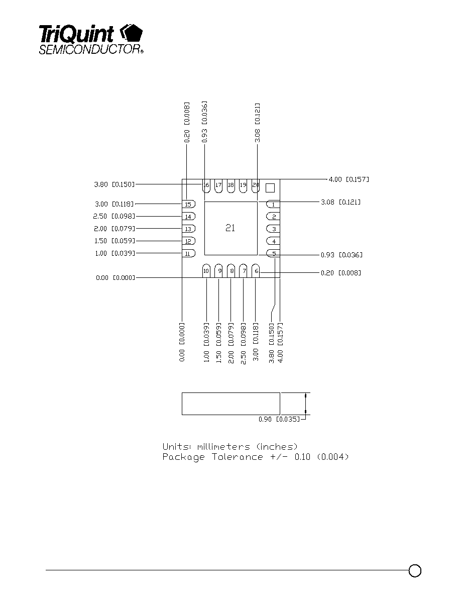
Mechanical Specifications
TGA2803-SM

Advance Product Information
July 20, 2005
7
TriQuint Semiconductor Texas: Phone (972)994-8465 Fax (972)994-8504 Email: Info-mmw@tqs.com Web: www.triquint.com
Pinout
Top Side
Dot indicates Pin 1
Bottom Side
Pin
Description
Pin
Description
1
RF Input 1
11
RF Output 2
2
RF Input 1
12
RF Output 2
3
GND
13, 21
GND
4
RF Input 2
14
RF Output 1
5
RF Input 2
15
RF Output 1
6
NC
16
NC
7
VG2 (Optional)
17
VDD (choked)
8
VDD
18
VDD
9
VDD (choked)
19
VG1 (Optional)
10
Isense 1/
20
NC
1/
Bias current monitor: I
bias
= V
Pin 10
/
TGA
2803
TGA2803-SM

Advance Product Information
July 20, 2005
8
TriQuint Semiconductor Texas: Phone (972)994-8465 Fax (972)994-8504 Email: Info-mmw@tqs.com Web: www.triquint.com
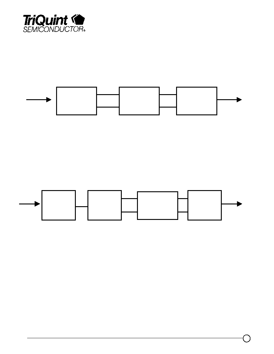
Optical Receiver
Electrical Gain Amplifier
Balun
TGA 2803
Push-Pull
TIA
Balun
Electrical Out
75
:
Electrical In
75
:
TGA2803-SM
Application Diagrams
Fiber In
Balun
Balun
Electrical Out
75
:
Photodiode
+
Transformer
TGA 2803
Push-Pull
TIA

Advance Product Information
July 20, 2005
9
TriQuint Semiconductor Texas: Phone (972)994-8465 Fax (972)994-8504 Email: Info-mmw@tqs.com Web: www.triquint.com
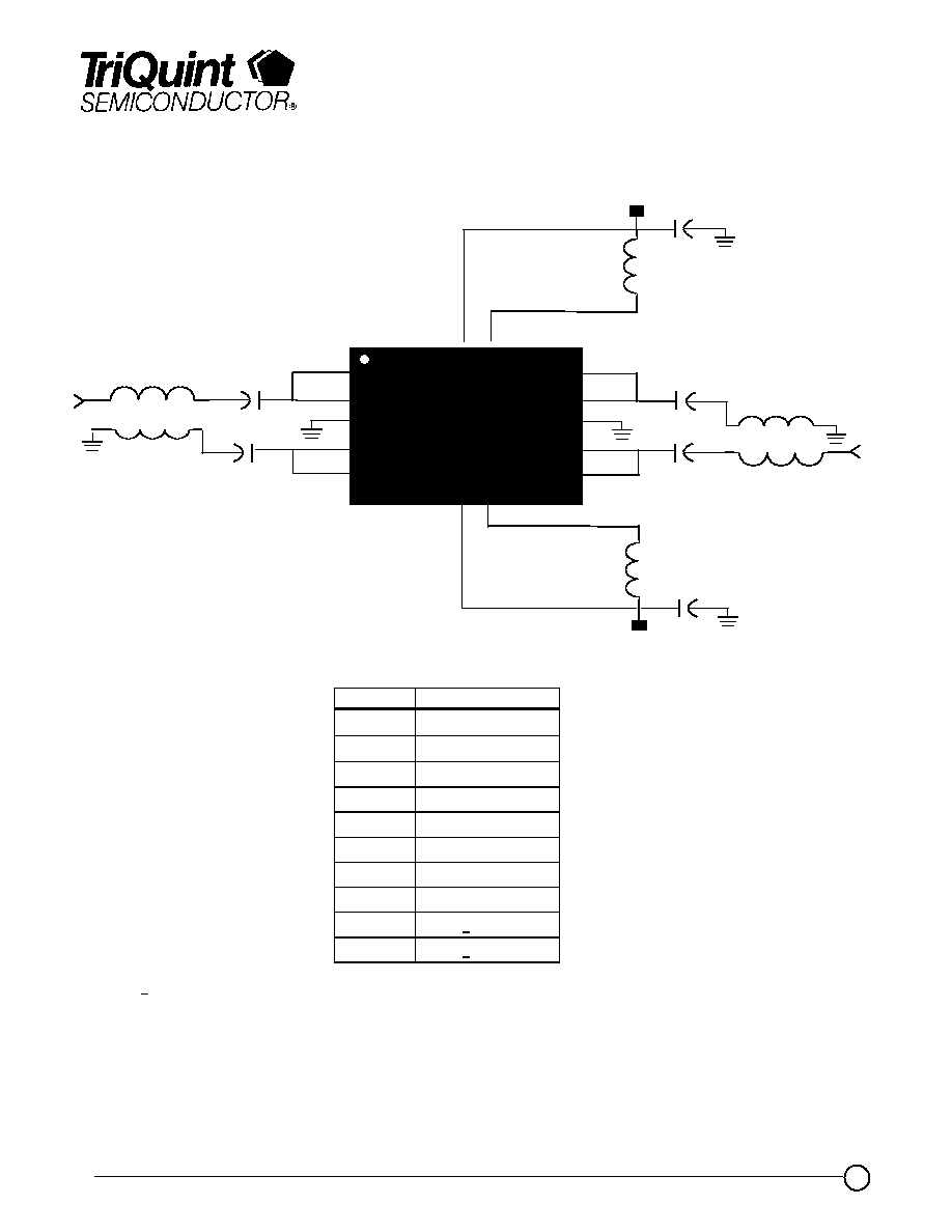
Recommended Electrical Assembly
Component Description
Ref
Description
C1
0.01
µ
F Capacitor
C2
0.01
µ
F Capacitor
C3
470pF Capacitor
C4
470pF Capacitor
C5
270pF Capacitor
C6
270pF Capacitor
L1
820nH Inductor
L2
820nH Inductor
T1
Balun 1/
T2
Balun 1/
1/
Balun performance impacts amplifier return losses and gain. Best performance can be
achieved by winding 34 or 36 gauge bifilar wire around a small binocular core made
from low-loss magnetic material. Suitable wire may be obtained from MWS Wire
Industries. Core vendors include Ferronics, Fairrite, TDK, and Micrometals.
Alternatively, off-the-shelf baluns can be purchased from a number of vendors
including Mini-Circuits (ADTL1-18-75), M/A-COM (ETC1-1-13), and Pulse Engineering
(CX2071).
+8V
+8V
RF
OUT
TGA 2803
1
2
3
4
5
15
14
13
12
11
6
7
8
9
10
20 19 18 17 16
RF
IN
T1
T2
L1
C2
C3
C4
C5
C6
C1
L2
TGA2803-SM

Advance Product Information
July 20, 2005
10
TriQuint Semiconductor Texas: Phone (972)994-8465 Fax (972)994-8504 Email: Info-mmw@tqs.com Web: www.triquint.com
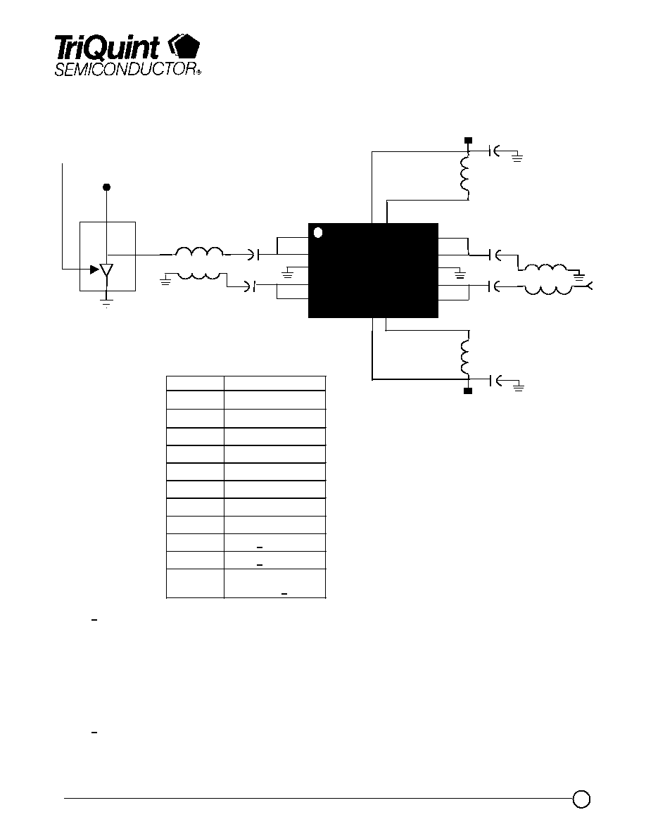
Component Description
Ref
Description
C1
0.01
µ
F Capacitor
C2
0.01
µ
F Capacitor
C3
470pF Capacitor
C4
470pF Capacitor
C5
270pF Capacitor
C6
270pF Capacitor
L1
820nH Inductor
L2
820nH Inductor
T1
Balun 1/
T2
Balun 1/
PD
Broadband
Photodiode 2/
1/
Balun performance impacts amplifier return losses and gain. Best
performance can be achieved by winding 34 or 36 gauge bifilar wire
around a small binocular core made from low-loss magnetic material.
Suitable wire may be obtained from MWS Wire Industries. Core vendors
include Ferronics, Fairrite, TDK, and Micrometals.
Alternatively, off-the-shelf baluns can be purchased from a number of
vendors including Mini-Circuits (ADTL1-18-75), M/A-COM (ETC1-1-13),
and Pulse Engineering (CX2071).
2/
Emcore 2609C Broadband Photodiode Module is recommended. The
module includes a 4:1 impedance transformer.
Recommended Electro-Optical Assembly
+8V
Single-Mode
Fiber
PD
-15V
RFout
+8V
RF
OUT
TGA 2803
1
2
3
4
5
15
14
13
12
11
6 7
8 9 10
20 19 18 17 16
T1
T2
L1
C2
C3
C4
C5
C6
C1
L2
TGA2803-SM

Advance Product Information
July 20, 2005
11
TriQuint Semiconductor Texas: Phone (972)994-8465 Fax (972)994-8504 Email: Info-mmw@tqs.com Web: www.triquint.com
Ordering Information
Part
Package Style
TGA2803-SM
QFN 20L 4x4 Surface Mount
Recommended Surface Mount Package Assembly
Proper ESD precautions must be followed while handling packages.
Clean the board with acetone. Rinse with alcohol. Allow the circuit to fully dry.
TriQuint recommends using a conductive solder paste for attachment. Follow solder paste and reflow oven
vendors' recommendations when developing a solder reflow profile. Typical solder reflow profiles are listed
in the table below.
Hand soldering is not recommended. Solder paste can be applied using a stencil printer or dot placement.
The volume of solder paste depends on PCB and component layout and should be well controlled to
ensure consistent mechanical and electrical performance.
Clean the assembly with alcohol.
GaAs MMIC devices are susceptible to damage from Electrostatic Discharge. Proper precautions should
be observed during handling, assembly and test.
Typical Solder Reflow Profiles
Reflow Profile
SnPb
Pb Free
Ramp-up Rate
3
∞
C/sec
3
∞
C/sec
Activation Time and
Temperature
60 ≠ 120 sec @ 140 ≠ 160
∞
C
60 ≠ 180 sec @ 150 ≠ 200
∞
C
Time above Melting Point
60 ≠ 150 sec
60 ≠ 150 sec
Max Peak Temperature
240
∞
C
260
∞
C
Time within 5
∞
C of Peak
Temperature
10 ≠ 20 sec
10 ≠ 20 sec
Ramp-down Rate
4 ≠ 6
∞
C/sec
4 ≠ 6
∞
C/sec
TGA2803-SM
