
Advance Product Information
September 16, 2003
1
Note: Devices designated as EPU are typically early in their characterization process prior to finalizing all electrical and process
specifications. Specifications are subject to change without notice.
TriQuint Semiconductor Texas Phone: (972)994-8465 Fax: (972)994 8504 Email: info-mmw@tqs.com Web: www.triquint.com
4 Watt 802.11a Packaged Amplifier TGA2921-EPU-SG
Key Features
∑
4.9 - 6 GHz Application Frequency Range
∑
11 dB Nominal Gain @ 8V 800mA
∑
36 dBm Nominal P1dB @ 8V 800mA
∑
IMD3 -50dBc @ 24dBm SCL, Typical
∑
Bias Conditions: 7-9 V @ 700-800 mA (Quiescent)
∑
0.5
µ
m HFET Technology
∑
2 lead Cu base SMT package
Fixtured Measured Performance
Bias Conditions: Vd = 8 V, Idq =800 mA
Performance data taken @ in a 5.75GHz application circuit
Primary Applications
∑
802.11a WLAN Bridge Amplifiers
∑
U-NII Band HPA
∑
C-Band Pt-Pt and Pt-Multi Pt Radio
The TGA2921-SG HPA provides 11
dB of gain and 4 W of output power
across 4.9 - 6 GHz. The device is
ideally suited for high linearity, high
power wireless data applications
such as 802.11a WLAN Bridge
Amplifiers, U-NII and Point-to-Point
or Point-to-Multi-Point Non-Line of
Sight radios. The surface mount
package has a high thermal
conductivity copper base. Internal
partial matching simplifies system
board layout by requiring a minimum
of external components.
Evaluation Boards are available.
Product Description
-12
-9
-6
-3
0
3
6
9
12
5
5.2
5.4
5.6
5.8
6
6.2
6.4
6.6
6.8
7
Frequency (GHz)
G
a
in (
d
B)
-20
-15
-10
-5
0
5
10
15
20
Retur
n
Loss (dB)
Gain
Input
Output
0
5
10
15
20
25
30
35
40
14
16
18
20
22
24
26
28
30
Pin (dBm)
Pout (dBm
) & Ga
in (dB)
0
200
400
600
800
1000
1200
1400
1600
IDS (m
A)
Gain
Pout
IDS

Advance Product Information
September 16, 2003
2
Note: Devices designated as EPU are typically early in their characterization process prior to finalizing all electrical and process
specifications. Specifications are subject to change without notice.
TriQuint Semiconductor Texas Phone: (972)994-8465 Fax: (972)994 8504 Email: info-mmw@tqs.com Web: www.triquint.com
TABLE I
MAXIMUM RATINGS 1/
Symbol
Parameter
Value
Notes
Vd
Drain Supply Voltage
10 V
2/
Vg
Gate Supply Voltage Range
0 V to -5 V
Idq
Drain Supply Current (Quiescent)
2 A
2/
| Ig |
Gate Current
38 mA
P
IN
Input Continuous W ave Power
30 dBm
2/
P
D
Power Dissipation
7.9 W
2/, 3/
T
CH
Operating Channel Temperature
175
∞
C
4/
T
M
Mounting Temperature (30 Seconds)
320
∞
C
T
STG
Storage Temperature
-65 to 150
∞
C
1/
These ratings represent the maximum operable values for this device.
2/
Combinations of supply voltage, supply current, input power, and output power shall not exceed P
D
.
3/
W hen operated at this bias condition with a base plate temperature of 85
0
C, the MTTF life is 2 E+8
hours.
4/ Junction operating temperature will directly affect the device median time to failure (T
M
).
For maximum life, it is recommended that junction temperatures be maintained at the lowest
possible levels.
TGA2921-EPU-SG

Advance Product Information
September 16, 2003
3
Note: Devices designated as EPU are typically early in their characterization process prior to finalizing all electrical and process
specifications. Specifications are subject to change without notice.
TriQuint Semiconductor Texas Phone: (972)994-8465 Fax: (972)994 8504 Email: info-mmw@tqs.com Web: www.triquint.com
TABLE III
THERMAL INFORMATION
Parameter
Test Conditions
T
CH
(
o
C)
R
JC
(
∞
C/W)
T
M
(HRS)
R
JC
Thermal
Resistance
(channel to backside
of package)
Vd = 8 V
I
D
= 800 mA
Pdiss = 6.4 W
155
11
1.6 E+9
Note: Package backside SnPb soldered to carrier at 85
∞
C baseplate temperature.
Worst case condition with no RF applied, 100% of DC power is dissipated.
TABLE II
RF CHARACTERIZATION TABLE
(T
A
= 25
∞
C, Nominal)
(Vd = 8 V, Idq = 800 mA)
SYMBOL
PARAMETER
TEST
CONDITION
TYPICAL
UNITS
Gain
Small Signal Gain
F = 5.75 GHz
11
dB
IRL
Input Return Loss
F = 5.75 GHz
12
dB
ORL
Output Return Loss
F = 5.75 GHz
7
dB
P1dB
Output Power @ P1dB
F = 5.75 GHz
36
dBm
TGA2921-EPU-SG
Advance Product Information
September 16, 2003
4
Note: Devices designated as EPU are typically early in their characterization process prior to finalizing all electrical and process
specifications. Specifications are subject to change without notice.
TriQuint Semiconductor Texas Phone: (972)994-8465 Fax: (972)994 8504 Email: info-mmw@tqs.com Web: www.triquint.com
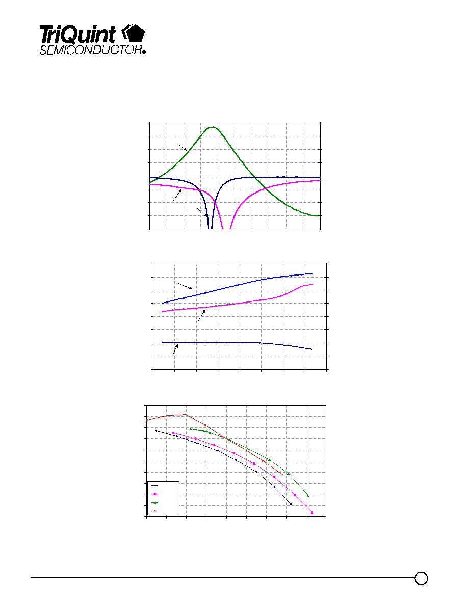
Bias Conditions: Vd = 7 V, Idq = 700 mA
Measured Fixtured Data
Application Circuit tuned to 5.75 GHz
25
30
35
40
45
50
55
60
65
70
75
12
14
16
18
20
22
24
26
28
30
Output Power per Tone (dBm)
IM
D3 level (dBc)
5.6GHz
5.7GHz
5.8GHz
5.9GHz
TGA2921-EPU-SG
-12
-9
-6
-3
0
3
6
9
12
5
5.2
5.4
5.6
5.8
6
6.2
6.4
6.6
6.8
7
Frequency (GHz)
Gain (dB)
-20
-15
-10
-5
0
5
10
15
20
Return Loss (dB)
Gain
Input
Output
0
5
10
15
20
25
30
35
40
14
16
18
20
22
24
26
28
30
Pin (dBm)
Pout (dB
m
) &
Ga
in (dB
)
0
200
400
600
800
1000
1200
1400
1600
IDS
(mA)
Gain
Pout
IDS

Advance Product Information
September 16, 2003
5
Note: Devices designated as EPU are typically early in their characterization process prior to finalizing all electrical and process
specifications. Specifications are subject to change without notice.
TriQuint Semiconductor Texas Phone: (972)994-8465 Fax: (972)994 8504 Email: info-mmw@tqs.com Web: www.triquint.com
Measured Fixtured Data
Application Circuit tuned to 5.75 GHz
Bias Conditions: Vd = 8 V, Idq = 800 mA
25
30
35
40
45
50
55
60
65
70
75
12
14
16
18
20
22
24
26
28
30
Output Power per Tone (dBm)
IM
D3 level (dBc)
5.6GHz
5.7GHz
5.8GHz
5.9GHz
TGA2921-EPU-SG
-12
-9
-6
-3
0
3
6
9
12
5
5.2
5.4
5.6
5.8
6
6.2
6.4
6.6
6.8
7
Frequency (GHz)
Gain (dB)
-20
-15
-10
-5
0
5
10
15
20
Return Loss (dB)
Gain
Input
Output
0
5
10
15
20
25
30
35
40
14
16
18
20
22
24
26
28
30
Pin (dBm)
Pout (dB
m
)
&
Ga
in (dB
)
0
200
400
600
800
1000
1200
1400
1600
IDS (mA)
Gain
Pout
IDS