Advance Product Information
September 16, 2003
1
Note: Devices designated as EPU are typically early in their characterization process prior to finalizing all electrical and process
specifications. Specifications are subject to change without notice.
TriQuint Semiconductor Texas Phone: (972)994-8465 Fax: (972)994 8504 Email: info-mmw@tqs.com Web: www.triquint.com
2 Watt 802.11a Packaged Amplifier TGA2922-EPU-SG
Key Features
∑
4.9 - 6 GHz Application Frequency Range
∑
11 dB Nominal Gain @ 8V 480mA
∑
34 dBm Nominal P1dB @ 8V 480mA
∑
IMD3 -50dBc @ 22dBm SCL, Typical
∑
Bias Conditions: 7-9 V @ 480 mA (Quiescent)
∑
0.5
µ
m HFET Technology
∑
2 lead Cu base SMT package
Fixtured Measured Performance
Bias Conditions: Vd = 8 V, Idq =480 mA
Performance data taken @ in a 5.75GHz
application circuit
Primary Applications
∑
802.11a WLAN Bridge Amplifiers
∑
U-NII Band HPA
∑
C-Band Pt-Pt and Pt-Multi Pt Radio
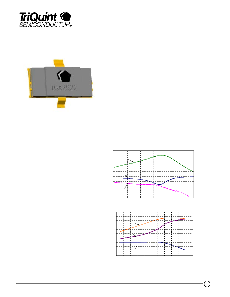
The TGA2922-SG HPA provides
11dB of gain and 2 W of output
power across 4.9 - 6 GHz. The
device is ideally suited for high
linearity, high power wireless data
applications such as 802.11a WLAN
Bridge Amplifiers, U-NII and Point-
to-Point or Point-to-Multi Point Non-
Line of Sight radios. The surface
mount package has a high thermal
conductivity copper base. Internal
partial matching simplifies system
board layout by requiring a minimum
of external components.
Evaluation Boards are available.
Product Description
0
4
8
12
16
20
24
28
32
36
40
9
11
13
15
17
19
21
23
25
27
29
31
Pin (dBm)
P
o
u
t
(d
Bm
) & Gain
(d
B)
300
400
500
600
700
800
IDS (m
A)
Pout
IDS
Gain
-12
-9
-6
-3
0
3
6
9
12
15
4
4.5
5
5.5
6
6.5
7
Frequency (GHz)
Gain (dB)
-20
-15
-10
-5
0
5
10
15
20
25
R
e
turn Loss (dB
)
Gain
Input
Output

Advance Product Information
September 16, 2003
2
Note: Devices designated as EPU are typically early in their characterization process prior to finalizing all electrical and process
specifications. Specifications are subject to change without notice.
TriQuint Semiconductor Texas Phone: (972)994-8465 Fax: (972)994 8504 Email: info-mmw@tqs.com Web: www.triquint.com
TABLE I
MAXIMUM RATINGS 1/
Symbol
Parameter
Value
Notes
Vd
Drain Supply Voltage
10 V
2/
Vg
Gate Supply Voltage Range
0 V to -5 V
Idq
Drain Supply Current (Quiescent)
1 A
2/
| Ig |
Gate Current
19 mA
P
IN
Input Continuous Wave Power
30 dBm
2/
P
D
Power Dissipation
4.1 W
2/, 3/
T
CH
Operating Channel Temperature
175
∞
C
4/
T
M
Mounting Temperature (30 Seconds)
320
∞
C
T
STG
Storage Temperature
-65 to 150
∞
C
1/
These ratings represent the maximum operable values for this device.
2/
Combinations of supply voltage, supply current, input power, and output power shall not exceed P
D
.
3/
When operated at this bias condition with a base plate temperature of 85
∞
C, the MTTF life is 2 E+8 hours.
4/ Junction operating temperature will directly affect the device median time to failure (T
M
). For maximum
life, it is recommended that junction temperatures be maintained at the lowest possible levels.
TGA2922-EPU-SG

Advance Product Information
September 16, 2003
3
Note: Devices designated as EPU are typically early in their characterization process prior to finalizing all electrical and process
specifications. Specifications are subject to change without notice.
TriQuint Semiconductor Texas Phone: (972)994-8465 Fax: (972)994 8504 Email: info-mmw@tqs.com Web: www.triquint.com
TABLE III
THERMAL INFORMATION
Parameter
Test Conditions
T
CH
(
o
C)
R
JC
(
∞
C/W)
T
M
(HRS)
R
JC
Thermal
Resistance
(channel to backside
of package)
Vd = 8 V
I
D
= 480 mA
Pdiss = 3.8 W
168
22
4 E+8
Note: Package backside SnPb soldered to carrier at 85
∞
C baseplate temperature.
Worst case condition with no RF applied, 100% of DC power is dissipated.
TABLE II
RF CHARACTERIZATION TABLE
(T
A
= 25
∞
C, Nominal)
(Vd = 8 V, Idq = 480 mA)
SYMBOL
PARAMETER
TEST
CONDITION
TYPICAL
UNITS
Gain
Small Signal Gain
F = 5.75 GHz
11
dB
IRL
Input Return Loss
F = 5.75 GHz
7
dB
ORL
Output Return Loss
F = 5.75 GHz
7
dB
P1dB
Output Power @ P1dB
F = 5.75 GHz
34
dBm
TGA2922-EPU-SG

Advance Product Information
September 16, 2003
4
Note: Devices designated as EPU are typically early in their characterization process prior to finalizing all electrical and process
specifications. Specifications are subject to change without notice.
TriQuint Semiconductor Texas Phone: (972)994-8465 Fax: (972)994 8504 Email: info-mmw@tqs.com Web: www.triquint.com
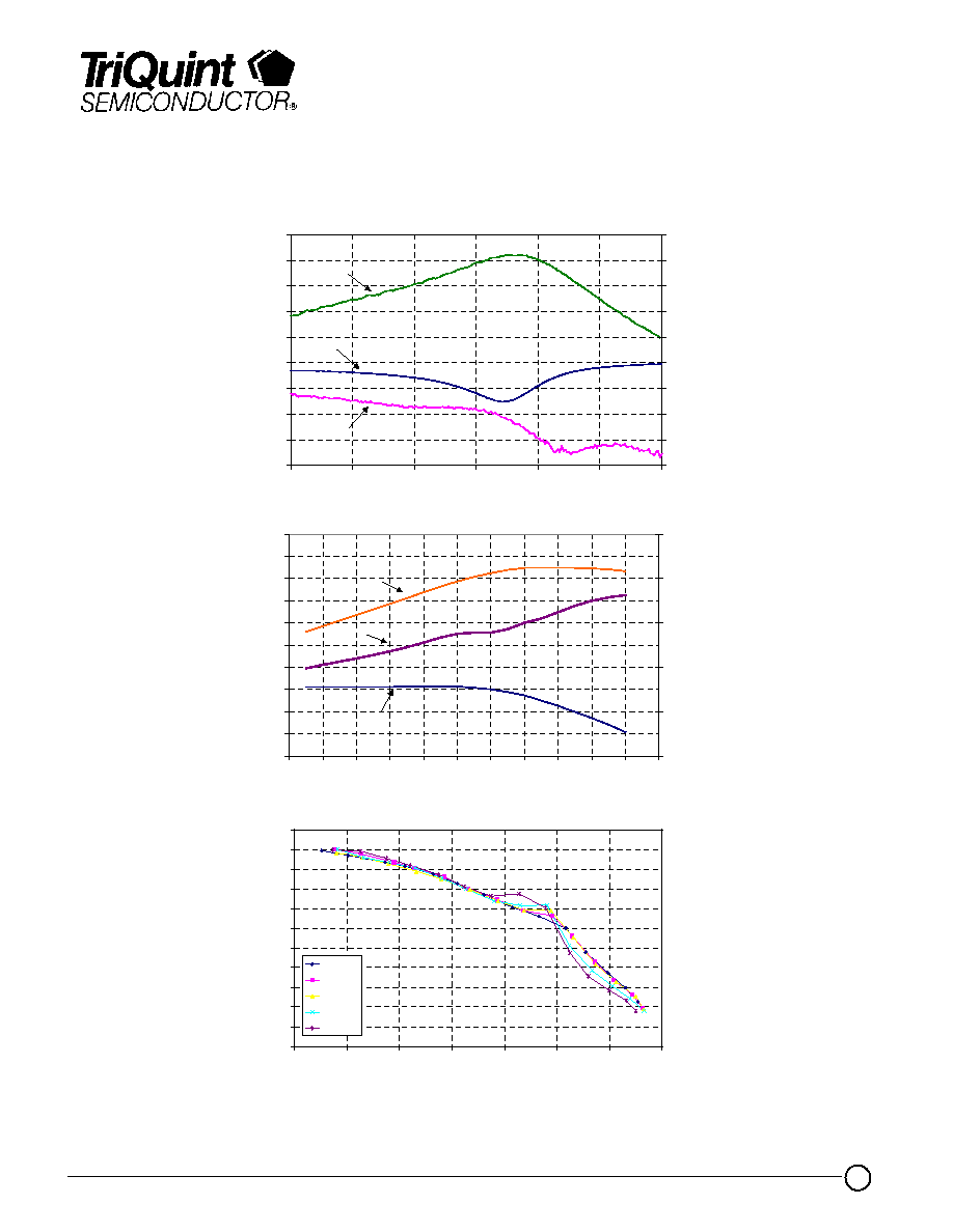
Bias Conditions: Vd = 7 V, Idq = 480 mA
Measured Fixtured Data
Application Circuit tuned to 5.75 GHz
TGA2922-EPU-SG
10
15
20
25
30
35
40
45
50
55
60
65
16
18
20
22
24
26
28
30
Output Power per tone (dBm)
IM
D3 (
d
Bc)
5.6GHz
5.7GHz
5.8GHz
5.9GHz
6.0GHz
0
4
8
12
16
20
24
28
32
36
40
9
11
13
15
17
19
21
23
25
27
29
31
Pin (dBm)
Po
u
t
(d
Bm) & Gain
(d
B)
300
400
500
600
700
800
IDS (mA)
Pout
IDS
Gain
-12
-9
-6
-3
0
3
6
9
12
15
4
4.5
5
5.5
6
6.5
7
Frequency (GHz)
G
ain (dB)
-20
-15
-10
-5
0
5
10
15
20
25
Return Loss (dB)
Gain
Input
Output

Advance Product Information
September 16, 2003
5
Note: Devices designated as EPU are typically early in their characterization process prior to finalizing all electrical and process
specifications. Specifications are subject to change without notice.
TriQuint Semiconductor Texas Phone: (972)994-8465 Fax: (972)994 8504 Email: info-mmw@tqs.com Web: www.triquint.com
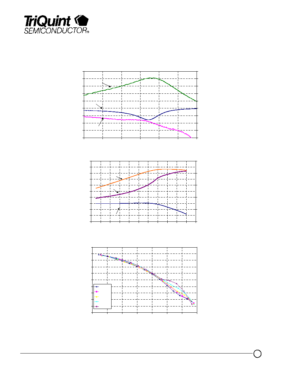
Measured Fixtured Data
Application Circuit tuned to 5.75 GHz
Bias Conditions: Vd = 8 V, Idq = 480 mA
TGA2922-EPU-SG
15
20
25
30
35
40
45
50
55
60
65
16
18
20
22
24
26
28
30
Output Power per tone (dBm)
IMD3 (dBc)
5.6GHz
5.7GHz
5.8GHz
5.9GHz
6.0GHz
0
4
8
12
16
20
24
28
32
36
40
9
11
13
15
17
19
21
23
25
27
29
31
Pin (dBm)
P
out (dBm
) & Gain (dB)
300
400
500
600
700
800
IDS
(m
A)
Pout
IDS
Gain
-12
-9
-6
-3
0
3
6
9
12
15
4
4.5
5
5.5
6
6.5
7
Frequency (GHz)
Gain (dB)
-20
-15
-10
-5
0
5
10
15
20
25
Ret
urn Loss (
d
B)
Gain
Input
Output
