 | ĐНокŃŃОннŃĐš кОПпОнонŃ: TGA4043 | ХкаŃĐ°ŃŃ:  PDF PDF  ZIP ZIP |
Äîęóěĺíňŕöč˙ č îďčńŕíč˙ www.docs.chipfind.ru

Advance Product Information
April 25, 2005
1
TriQuint Semiconductor Texas Phone: (972)994-8465 Fax: (972)994 8504 Email: info-mmw@tqs.com Web: www.triquint.com
Q-band Power Amplifier
TGA4043
Key Features
ˇ
Frequency Range: 40-45 GHz
ˇ
29 dBm Nominal Pout @ P1dB
ˇ
10 dB Nominal Gain
ˇ
0.25 um pHEMT Technology
ˇ
Bias 7V @ 500 mA
ˇ
Chip Dimensions 3.08 mm x 3.14 x 0.10 mm
(0.121 x 0.124 x 0.004 in)
Primary Applications
ˇ
Point to Point Radio
ˇ
Point to Multipoint Radio
ˇ
Military Communications
Measured Fixtured Data
Bias Conditions: Vd = 7V, Id = 500mA
25
26
27
28
29
30
31
32
40
40.5
41
41.5
42
42.5
43
43.5
44
44.5
45
Frequency (GHz)
P1d
B
(
d
Bm
)
Product Description
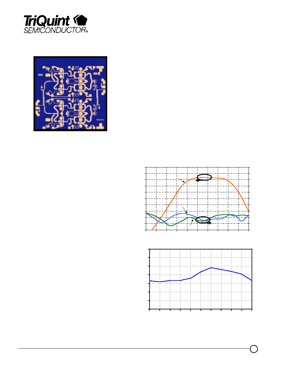
The TriQuint TGA4043 is a compact High
Power Amplifier MMIC for Q-band
applications. The part is designed using
TriQuint's proven standard 0.25 um gate
power pHEMT production process.
The TGA4043 provides a nominal 28
dBm of output power at 1 dB gain
compression from 40-45 GHz with a small
signal gain of 10 dB.
The part is ideally suited for low cost
emerging markets such as Point-to-Point
Radio and Point-to-Multi Point
Communications.
The TGA4043 is 100% DC and RF tested
on-wafer to ensure performance
compliance.
-15
-12
-9
-6
-3
0
3
6
9
12
15
30
32
34
36
38
40
42
44
46
48
50
Frequency (GHz)
G
a
in (
d
B)
-25
-20
-15
-10
-5
0
5
10
15
20
25
Retur
n
Loss (dB)
Input
Output
Gain
Note: This device is early in the characterization process prior to finalizing all electrical specifications. Specifications are subject to
change without notice.

Advance Product Information
April 25, 2005
2
TriQuint Semiconductor Texas Phone: (972)994-8465 Fax: (972)994 8504 Email: info-mmw@tqs.com Web: www.triquint.com
TABLE I
MAXIMUM RATINGS 1/
SYMBOL
PARAMETER
VALUE
NOTES
V
+
Positive Supply Voltage
8 V
2/
V
-
Negative Supply Voltage Range
-5V TO 0V
I
+
Positive Supply Current
960 mA
2/
| I
G
|
Gate Supply Current
56 mA
P
IN
Input Continuous Wave Power
27 dBm
2/
P
D
Power Dissipation
4.6 W
2/, 3/
T
CH
Operating Channel Temperature
150
°
C
4/, 5/
T
M
Mounting Temperature (30 Seconds)
320
°
C
T
STG
Storage Temperature
-65 to 150
°
C
1/
These ratings represent the maximum operable values for this device.
2/
Current is defined under no RF drive conditions. Combinations of supply voltage, supply
current, input power, and output power shall not exceed P
D
.
3/
When operated at this power dissipation with a base plate temperature of 70
°
C, the median
life is 1 E+6 hours.
4/
Junction operating temperature will directly affect the device median time to failure (T
M
). For
maximum life, it is recommended that junction temperatures be maintained at the lowest
possible levels.
5/
These ratings apply to each individual FET.
TGA4043
TABLE II
DC PROBE TEST
(T
A
= 25
°
C, Nominal)
SYMBOL
PARAMETER
MINIMUM
MAXIMUM
UNIT
I
dss, Q1
Saturated Drain Current
40
188
mA
G
m, Q1
Transconductance
88
212
mS
V
p, Q1,2, 3-6, 7, 8, 9-12
Pinch-off Voltage
-1.5
-0.5
V
V
BVGD, Q1,2
Breakdown Voltage Gate-
Drain
-30
-8
V
V
BVGS, Q1
Breakdown Voltage Gate-
Source
-30
-8
V

Advance Product Information
April 25, 2005
3
TriQuint Semiconductor Texas Phone: (972)994-8465 Fax: (972)994 8504 Email: info-mmw@tqs.com Web: www.triquint.com
TABLE III
RF CHARACTERIZATION TABLE
(T
A
= 25
°
C, Nominal)
Vd = 7V, Id = 500 mA
SYMBOL
PARAMETER
TEST
CONDITION
TYPICAL
LIMITS
UNITS
Gain
Small Signal Gain
F = 40-45 GHz
10
dB
IRL
Input Return Loss
F = 40-45 GHz
14.5
dB
ORL
Output Return Loss
F = 40-45 GHz
12.5
dB
P
1dB
Output Power @
1dB Gain
Compression
F = 40-45 GHz
29
dBm
TABLE IV
THERMAL INFORMATION*
Parameter
Test Conditions
T
CH
(
o
C)
R
T
JC
(
q
C/W)
T
M
(HRS)
R
JC
Thermal
Resistance
(channel to backside of
carrier)
Vd = 7 V
I
D
= 500 mA
Pdiss = 3.5 W
130
17.3
5.9 E+6
Note: Assumes eutectic attach using 1.5 mil 80/20 AuSn mounted to a 20 mil
CuMo Carrier at 70
°
C baseplate temperature. Worst case condition with no RF
applied, 100% of DC power is dissipated.
TGA4043

Advance Product Information
April 25, 2005
4
TriQuint Semiconductor Texas Phone: (972)994-8465 Fax: (972)994 8504 Email: info-mmw@tqs.com Web: www.triquint.com
25
26
27
28
29
30
31
32
40
40.5
41
41.5
42
42.5
43
43.5
44
44.5
45
Frequency (GHz)
P1dB (dBm)
Measured Fixtured Data
Bias Conditions: Vd = 7V, Id = 500mA
15
17
19
21
23
25
27
29
31
6
8
10
12
14
16
18
20
22
24
Input power (dBm)
Out
put
power (
d
Bm)
40 GHz
41 GHz
42 GHz
43 GHz
44 GHz
45 GHz
-15
-12
-9
-6
-3
0
3
6
9
12
15
30
32
34
36
38
40
42
44
46
48
50
Frequency (GHz)
G
a
in (
d
B)
-25
-20
-15
-10
-5
0
5
10
15
20
25
Retur
n
Loss (dB)
Input
Output
Gain
0
2
4
6
8
10
12
14
16
6
8
10
12
14
16
18
20
22
24
Input power (dBm)
PAE (%)
40 GHz
41 GHz
42 GHz
43 GHz
44 GHz
45 GHz
TGA4043

Advance Product Information
April 25, 2005
5
TriQuint Semiconductor Texas Phone: (972)994-8465 Fax: (972)994 8504 Email: info-mmw@tqs.com Web: www.triquint.com
Mechanical Characteristics
GaAs MMIC devices are susceptible to damage from Electrostatic Discharge. Proper precautions should
be observed during handling, assembly and test.
!
'
Ă
$
!%Ă$
($$Ă"'
!%&!Ă $
'&%Ă&#
#
!
&
Ă
&
'
%
Ă
"
!
#
(
"
Ă
$
(
!
"
&
Ă
(
"
!
$
!
Ă
(
(
!
(
#
%
Ă
%
"
&
%
Ă
!
'
%
Ă
"
!
" #Ă !#
#
!
Ă
&
#
(
"
Ă
$
(
!
"
%
&
Ă
(
"
!
$
!
Ă
(
(
7qĂQhqĂĆ ĂSAĂDĂĂĂĂĂĂ
7qĂQhqĂĆ!ĂWtĂ ĂĂĂĂĂĂĂĂĂĂĂĂ
7qĂQhqĂĆ"ĂWqĂ ĂĂĂĂĂĂĂĂĂĂĂĂ
7qĂQhqĂĆ#ĂWtĂ ĂĂĂĂĂĂĂĂĂĂĂĂ
7qĂQhqĂĆ$ĂWqĂ ĂĂĂĂĂĂĂĂĂĂĂĂ
7qĂQhqĂĆ%Ă7hĂĂĂĂĂĂĂ
7qĂQhqĂĆ&ĂSAĂPĂĂ
7qĂQhqĂĆ'Ă7hĂĂĂĂĂĂĂ
7qĂQhqĂĆ(ĂWqĂ!ĂĂĂĂĂĂĂĂĂĂĂ
7qĂQhqĂĆ ĂWtĂ!ĂĂĂĂĂĂĂĂĂ
7qĂQhqĂĆ ĂWqĂĆ!ĂĂĂĂĂĂĂ
7qĂQhqĂĆ !ĂWtĂĆ!ĂĂĂĂĂĂĂ
Vv)ĂvyyvrrĂvpur
Uuvpxr)Ă Ă#ĂrsrrprĂy
8uvĂrqtrĂĂiqĂhqĂqvrvĂhrĂuĂĂprrĂsĂiqĂhq
8uvĂvrĂyrhpr)ĂĂ$ Ă!
BI9ĂDTĂ768FTD9@ĂPAĂHHD8
$ĂĂ "Ă#ĂĂ$
$ĂĂ $Ă#ĂĂ#
$ĂĂ $Ă#ĂĂ#
$ĂĂ $Ă#ĂĂ#
$ĂĂ $Ă#ĂĂ#
$ĂĂ $Ă#ĂĂ#
$ĂĂ "Ă#ĂĂ$
$ĂĂ "Ă#ĂĂ$
$ĂĂ $Ă#ĂĂ#
$ĂĂ $Ă#ĂĂ#
$ĂĂ $Ă#ĂĂ#
$ĂĂ $Ă#ĂĂ#
TGA4043
