Product Data Sheet
July 22, 2003
1
TriQuint Semiconductor Texas Phone: (972)994-8465 Fax: (972)994 8504 Email: info-mmw@tqs.com Web: www.triquint.com
K Band High Power Amplifier
TGA4502-SCC
Key Features
∑
17-27 GHz Application Frequency Range
∑
22 dB Nominal Gain
∑
29 dBm Nominal P1dB
∑
37dBm Nominal OTOI
∑
15 dB Nominal Return Loss
∑
0.25 um pHEMT 2MI Technology
∑
Bias 7V @ 760 mA
∑
Chip Dimensions 1.52 x 3.29 x .1mm
Primary Applications
∑
K Band Sat-Com
∑
Point-to-Point Radio
∑
Point-to-Multipoint Communications
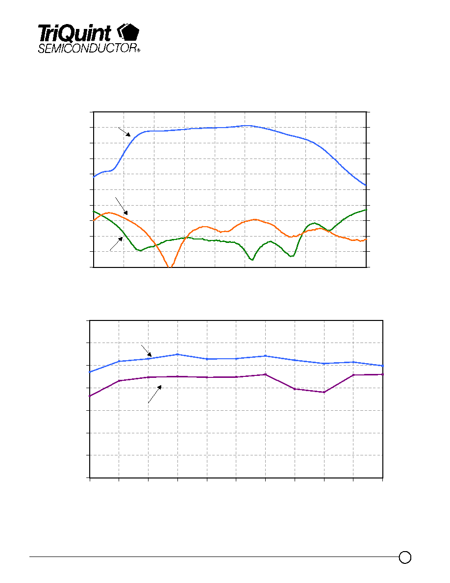
Fixtured Measured Performance
Bias Conditions: Vd = 7V, Id = 760mA
21
23
25
27
29
31
33
35
17
18
19
20
21
22
23
24
25
26
27
Frequency (GHz)
P1
dB (dBm
)
Psat
P1dB
-30
-24
-18
-12
-6
0
6
12
18
24
30
14
16
18
20
22
24
26
28
30
32
Frequency (G H z)
Ga
in
(d
B
)
-30
-24
-18
-12
-6
0
6
12
18
24
30
R
e
tu
r
n
L
o
s
s
(d
B
)
G ain
Inpu
t
Output
Product Description
The TriQuint TGA4502-SCC is a compact
High Power Amplifier MMIC for K-band
applications. The part is designed using
TriQuint's proven standard 0.25 um gate
power pHEMT production process.
The TGA4502-SCC provides a nominal
29 dBm of output power at 1 dB gain
compression from 17-27 GHz with a small
signal gain of 22 dB.
The part is ideally suited for low cost
emerging markets such as K-band
Satellite Communications, Point-to-Point
Radio, and Point-to-Multi Point
Communications.
The TGA4502-SCC is 100% DC and RF
tested on-wafer to ensure performance
compliance.
t

Product Data Sheet
July 22, 2003
2
TriQuint Semiconductor Texas Phone: (972)994-8465 Fax: (972)994 8504 Email: info-mmw@tqs.com Web: www.triquint.com
TGA4502-SCC
TABLE I
MAXIMUM RATINGS 1/
SYMBOL
PARAMETER
VALUE
NOTES
V
+
Positive Supply Voltage
8 V
2/
V
-
Negative Supply Voltage Range
-5V TO 0V
I
+
Positive Supply Current
880 mA
2/
| I
G
|
Gate Supply Current
28 mA
P
IN
Input Continuous Wave Power
26 dBm
2/
P
D
Power Dissipation
5.3 W
2/, 3/
T
CH
Operating Channel Temperature
150
∞
C
4/, 5/
T
M
Mounting Temperature (30 Seconds)
320
∞
C
T
STG
Storage Temperature
-65 to 150
∞
C
1/
These ratings represent the maximum operable values for this device.
2/
Current is defined under no RF drive conditions. Under RF drive, the supply current may rise to
1100 mA without damage. Combinations of supply voltage, supply current, input power, and
output power shall not exceed P
D
.
3/
When operated at this power dissipation with a base plate temperature of 70
∞
C, the median life is
1 E+6 hours.
4/
Junction operating temperature will directly affect the device median time to failure (T
M
). For
maximum life, it is recommended that junction temperatures be maintained at the lowest possible
levels.
5/
These ratings apply to each individual FET.

Product Data Sheet
July 22, 2003
3
TriQuint Semiconductor Texas Phone: (972)994-8465 Fax: (972)994 8504 Email: info-mmw@tqs.com Web: www.triquint.com
TABLE II
DC PROBE TEST
(T
A
= 25
∞
C, Nominal)
SYMBOL
PARAMETER
MINIMUM
MAXIMUM
UNIT
I
dss, Q1
Saturated Drain Current
60
282
mA
G
m, Q1
Transconductance
132
318
mS
V
p, Q1,2, 3-6, 7-10
Pinch-off Voltage
-1.5
-0.5
V
V
BVGD, Q1-10
Breakdown Voltage Gate-Drain
-30
-13
V
V
BVGS, Q1,2,3-6,7-10
Breakdown Voltage Gate-Source
-30
-13
V
Note: Q1 & Q2 are 600 um FETs. Q3-6 & Q7-10 are 2400 um FETs. Q1-10 is a 6000 um FET.
TGA4502-SCC
TABLE III
RF CHARACTERIZATION TABLE
(T
A
= 25
∞
C, Nominal)
Vd = 7V, Id = 760 mA
LIMITS
SYMBOL
PARAMETER
TEST
CONDITION
MINIMUM
TYPICAL
MAXIMUM
UNITS
Gain
Small Signal Gain
F = 17 ≠ 18 GHz
F = 17.5, 18 GHz
F = 20, 22, 24 GHz
F = 26.5 GHz
F = 27 GHz
--
17
18
17
--
22
--
23
--
20
--
--
--
--
--
dB
IRL
Input Return Loss
F = 17 ≠ 27 GHz
F = 17.5, 18, 20,
22, 24 GHz
F = 26.5 GHz
--
--
--
20
--
--
--
12
10
dB
ORL
Output Return Loss
F = 17 ≠ 27 GHz
F = 17.5, 18, 20,
22, 24 GHz
F = 26.5 GHz
--
--
--
15
--
--
--
12
10
dB
P
1dB
Output Power @
1dB Gain
Compression
F = 17 ≠ 27 GHz
F = 18, 26.5 GHz
--
27
30
--
--
dBm
OTOI *
Output Third Order
Intercept
F = 17 ≠ 27 GHz
F = 18, 26 GHz
--
34.5
37
--
--
--
dBm
* Pin/tone = -7dBm, Separation = 0.010 GHz

Product Data Sheet
July 22, 2003
4
TriQuint Semiconductor Texas Phone: (972)994-8465 Fax: (972)994 8504 Email: info-mmw@tqs.com Web: www.triquint.com
TABLE IV
THERMAL INFORMATION
Parameter
Test Conditions
T
CH
(
o
C)
R
JC
(
∞
C/W)
T
M
(HRS)
R
JC
Thermal
Resistance
(channel to backside of
carrier)
Vd = 7 V
Id = 760 mA
Pdiss = 5.3 W
150
15.1
1 E+6
Note: Assumes eutectic attach using 1.5 mil 80/20 AuSn mounted to a 20 mil
CuMo Carrier at 70
o
C baseplate temperature. Worst case condition with no RF
applied, 100% of DC power is dissipated.
TGA4502-SCC

Product Data Sheet
July 22, 2003
5
TriQuint Semiconductor Texas Phone: (972)994-8465 Fax: (972)994 8504 Email: info-mmw@tqs.com Web: www.triquint.com
TGA4502-SCC
21
23
25
27
29
31
33
35
17
18
19
20
21
22
23
24
25
26
27
Frequency (GHz)
P1dB (dBm)
Psat
P1dB
-30
-24
-18
-12
-6
0
6
12
18
24
30
14
16
18
20
22
24
26
28
30
32
Frequency (GHz)
Gain (dB)
-30
-24
-18
-12
-6
0
6
12
18
24
30
Return Loss (dB)
Gain
Inpu
t
Output
Measured Fixtured Data
Bias Conditions: Vd = 7V, Id = 760mA
t

Product Data Sheet
July 22, 2003
6
TriQuint Semiconductor Texas Phone: (972)994-8465 Fax: (972)994 8504 Email: info-mmw@tqs.com Web: www.triquint.com
Measured Fixtured Data
Bias Conditions: Vd = 7V, Id = 760mA
34
35
36
37
38
39
40
18
20
22
24
26
Frequency (GHz)
OTO
I
(dB
m
)
0
10
20
30
40
50
60
70
10
12
14
16
18
20
22
24
26
Pout/Tone (dBm)
IM
D3 & IM
D5 (dB
c
)
IMD5 @ 22GHz
IMD3 @ 22GHz
TGA4502-SCC

Product Data Sheet
July 22, 2003
7
TriQuint Semiconductor Texas Phone: (972)994-8465 Fax: (972)994 8504 Email: info-mmw@tqs.com Web: www.triquint.com
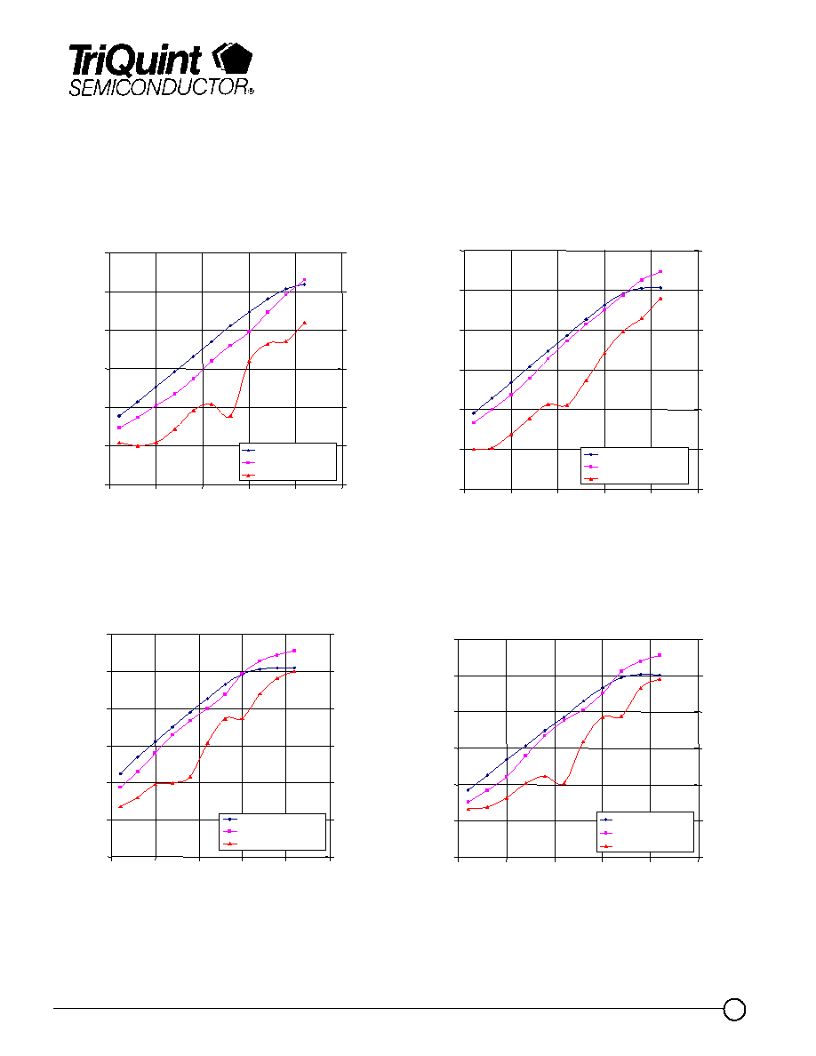
Measured Fixtured Data
Bias Conditions: Vd = 7V, Id = 760mA
At Frequency: 18GHz
0
5
10
15
20
25
30
-15
-10
-5
0
5
10
Pin (dBm)
Pout/to
n
e (dBm
)
-70
-55
-40
-25
-10
5
20
IM
D
3
& IM
D
5
(dBm)
Single Tone Power
IMD3
IMD5
At Frequency: 20GHz
0
5
10
15
20
25
30
-15
-10
-5
0
5
10
Pin (dBm)
Pout/to
n
e (dBm
)
-70
-55
-40
-25
-10
5
20
IM
D
3
& IM
D
5
(dBm)
Single Tone Power
IMD3
IMD5
At Frequency: 24GHz
0
5
10
15
20
25
30
-15
-10
-5
0
5
10
Pin (dBm)
Pout/to
n
e (dBm
)
-
70
-55
-40
-25
-10
5
20
IM
D
3
& IM
D
5
(dBm)
Single Tone Power
IMD3
IMD5
At Frequency: 26GHz
0
5
10
15
20
25
30
-15
-10
-5
0
5
10
Pin (dBm)
Pout/to
n
e (dBm
)
-70
-55
-40
-25
-10
5
20
IM
D
3
& IM
D
5
(dBm
)
Single Tone Power
IMD3
IMD5
TGA4502-SCC

Product Data Sheet
July 22, 2003
8
TriQuint Semiconductor Texas Phone: (972)994-8465 Fax: (972)994 8504 Email: info-mmw@tqs.com Web: www.triquint.com
GaAs MMIC devices are susceptible to damage from Electrostatic Discharge. Proper precautions should
be observed during handling, assembly and test.
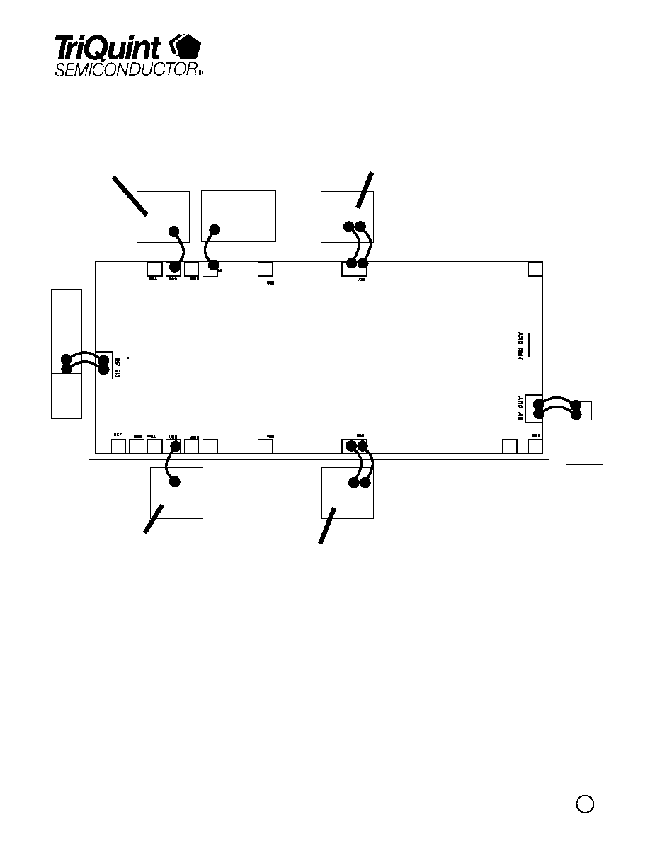
Recommended Assembly Diagram
TGA4502-SCC
Notes:
1. Connection to power det, ref
diode not shown.
2. 0.1
µ
F cap on gate, drain lines
not shown but required.
3. For high power operation,
gate voltage is recommended
from both sides.
4. Drain voltage is required
from both sides for Id > 780mA.
Vg
Vd
Output
TFN
100pF
100pF
Input
TFN
100pF
Vg (one side optional)
0.01
µ
F
DQ cap
(opt.)
Vd (one side optional for Id < 780 mA)
100pF

Product Data Sheet
July 22, 2003
9
TriQuint Semiconductor Texas Phone: (972)994-8465 Fax: (972)994 8504 Email: info-mmw@tqs.com Web: www.triquint.com
TGA4502 built-in power detector
On-chip diode functions as envelope detector
External coupler and DC bias required
External coupler
(-20dB)
TGA4502
50
C=2pF
Video out
(V
det
)
10K
External
DC bias
RF
OUT
RF
OUT
V
bias
100pF
100pF
TGA4502 with external test coupler
(amplifier bias connections not shown)
V
det
RF
IN
RF
OUT
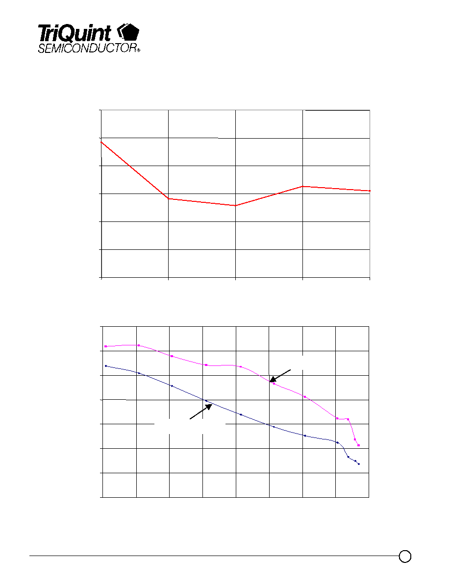
TGA4502 measured detector voltage offset vs output power
with 20dB coupler: Vb=0.8V, f = 20GHz, Coupler loss is
uncalibrated, 10K
load
0.01
0.1
1
10
8
10
12
14
16
18
20
22
24
26
28
30
32
Pout (dBm)
D
e
t
ect
or
v
o
l
t
a
g
e (
V
)
TGA4502-SCC

Product Data Sheet
July 22, 2003
10
TriQuint Semiconductor Texas Phone: (972)994-8465 Fax: (972)994 8504 Email: info-mmw@tqs.com Web: www.triquint.com
Mechanical Drawing
GaAs MMIC devices are susceptible to damage from Electrostatic Discharge. Proper precautions should
be observed during handling, assembly and test.
TGA4502-SCC
1.89
8
(
0
.075
)
1.89
8
(
0
.075
)
0.000
0.686
(0.027)
0.00
0
0.61
0
(
0
.024
)
0.87
5
(
0
.034
)
0.833
(0.033)
0.22
0
(
0
.009
)
3.18
8
(
0
.126
)
0.098
(.004)
3.00
4
(
0
.118
)
0.373
(0.015)
1.524
(0.060)
3.28
6
(
0
.129
)
0.61
2
(
0
.024
)
0.87
5
(
0
.034
)
0.09
5
(
0
.004
)
3.13
6
(
0
.123
)
1.26
2
(
0
.050
)
1.26
2
(
0
.046
)
1
8
3
4
5
6
7
2
9
10
11
12
13
14
15
Bond pad #1
(RF Input)
0.200 x 0.100 (0.008 x 0.004)
Bond pad #2
(RF Output)
0.200 x 0.100 (0.008 x 0.004)
Bond pad #3
VG2
0.100 x 0.100 (0.004 x 0.004)
Bond pad #4
DQ
0.100 x 0.100 (0.004 x 0.004)
Bond pad #5
VG3
0.100 x 0.100 (0.004 x 0.004)
Bond pad #6
VD3
0.180 x 0.100 (0.007 x 0.004)
Bond pad #7
DET OUT
0.100 x 0.100 (0.004 x 0.004)
Bond pad #8
PWR DET
0.175 x 0.100 (0.007 x 0.004)
Bond pad #9
REF2 0.100 x 0.100 (0.004 x 0.004)
Bond pad #10
REF1 0.100 x 0.100 (0.004 x 0.004)
Bond pad #11
VD3 0.180 x 0.100 (0.007 x 0.004)
Bond pad #12
VG3 0.100 x 0.100 (0.004 x 0.004)
Bond pad #13
DQ 0.100 x 0.100 (0.004 x 0.004)
Bond pad #14
VG2 0.100 x 0.100 (0.004 x 0.004)
Bond pad #15
REF3 0.100 x 0.100 (0.004 x 0.004)
Units: Millimeters (inches)
Thickness: 0.100 (0.004) (reference only)
Chip edge to bond pad dimensions are shown to center of bond pad
Chip size tolerance +/- 0.051 (0.002)
GND IS BACKSIDE OF MMIC
1.382
(0.544)

Product Data Sheet
July 22, 2003
11
TriQuint Semiconductor Texas Phone: (972)994-8465 Fax: (972)994 8504 Email: info-mmw@tqs.com Web: www.triquint.com
Assembly Process Notes
GaAs MMIC devices are susceptible to damage from Electrostatic Discharge. Proper precautions should
be observed during handling, assembly and test.
Reflow process assembly notes:
∑
Use AuSn (80/20) solder with limited exposure to temperatures at or above 300
∞
C
(for 30 sec max).
∑
An alloy station or conveyor furnace with reducing atmosphere should be used.
∑
No fluxes should be utilized.
∑
Coefficient of thermal expansion matching is critical for long-term reliability.
∑
Devices must be stored in a dry nitrogen atmosphere.
Component placement and adhesive attachment assembly notes:
∑
Vacuum pencils and/or vacuum collets are the preferred method of pick up.
∑
Air bridges must be avoided during placement.
∑
The force impact is critical during auto placement.
∑
Organic attachment can be used in low-power applications.
∑
Curing should be done in a convection oven; proper exhaust is a safety concern.
∑
Microwave or radiant curing should not be used because of differential heating.
∑
Coefficient of thermal expansion matching is critical.
Interconnect process assembly notes:
∑
Thermosonic ball bonding is the preferred interconnect technique.
∑
Force, time, and ultrasonics are critical parameters.
∑
Aluminum wire should not be used.
∑
Discrete FET devices with small pad sizes should be bonded with 0.0007-inch wire.
∑
Maximum stage temperature is 200
∞
C.
TGA4502-SCC
Die are shipped in H20-074149 waffle packs.


