 | –≠–ª–µ–∫—Ç—Ä–æ–Ω–Ω—ã–π –∫–æ–º–ø–æ–Ω–µ–Ω—Ç: TGA4811 | –°–∫–∞—á–∞—Ç—å:  PDF PDF  ZIP ZIP |
Advance Product Information
June 30, 2005
1
TriQuint Semiconductor Texas Phone: (972)994 8465 Fax: (972)994 8504 Web: www.triquint.com Info:
info-mmw@tqs.com
DC - 60 GHz Low Noise Amplifier TGA4811
Key Features
∑
60 GHz Bandwidth
∑
3.0 dB noise figure
∑
> 15 dB small signal gain
∑
13 dBm P1dB
∑
+/- 7 ps group delay variation
∑
Bias: 6V, 50 mA
∑
0.15 um 3MI mHEMT Technology
∑
Chip Dimensions: 1.30 x 1.06 x 0.1 mm
(0.051 x 0.042 x 0.004) in
Primary Applications
∑
Wideband LNA / gain block
∑
Test Equipment
∑
40 Gb/s optical networks
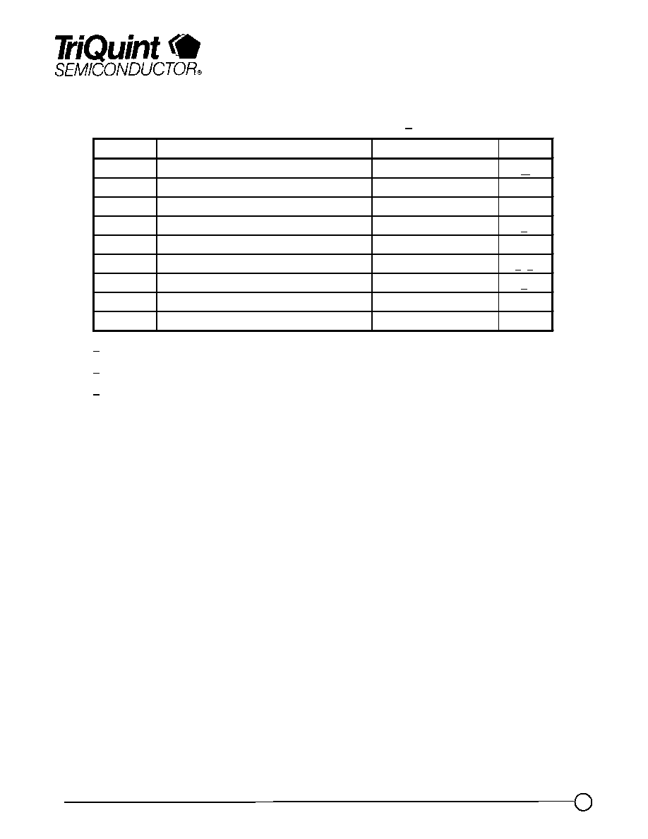
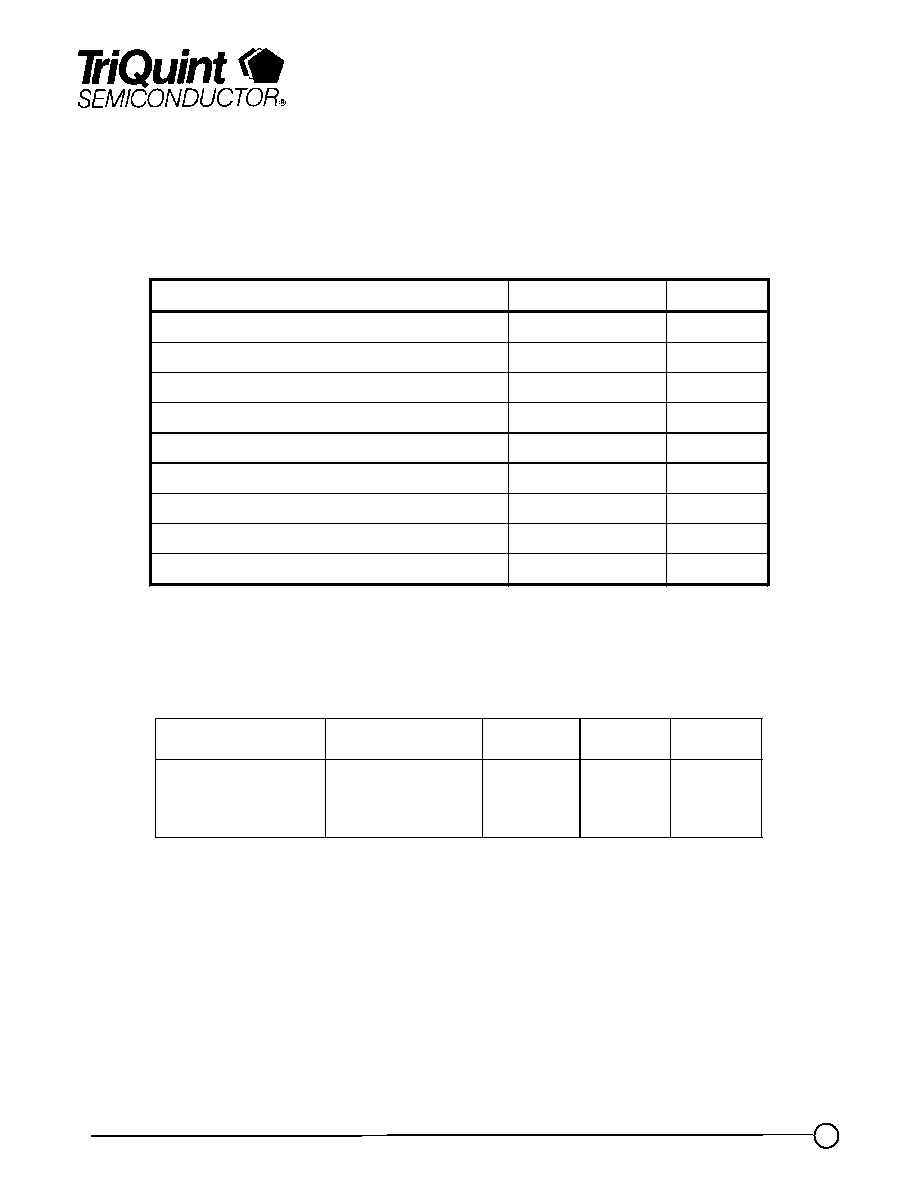
Measured Data
Bias Conditions: Vd = 6 V, Id = 50 mA
Note: This device is early in the characterization process prior to finalizing all electrical specifications. Specifications are subject to
change without notice.
0
2
4
6
8
10
12
14
16
0
5
10
15
20
25
30
35
40
45
50
Frequency (GHz)
Output P1dB (dBm)
0
2
4
6
8
10
12
14
16
Noise Figure (dB)
NF at 4.5V,42 mA
P1dB at 4.5V,42 mA
P1dB at 6V,52 mA
Description
The TriQuint TGA4811 is a DC - 60
GHz low noise amplifier that typically
provides 15 dB small signal gain and
input and output return loss is <10dB.
Normal Noise Figure is 3.0 dB from 2
- 40 GHz. P1dB is 13 dBm.
The TGA4811 is an excellent choice
for Test Equipment, 40Gb/s optical
network applications, and general
wideband LNA and Gain Block
applications
.
The TGA4811 is 100% RF tested to
ensure performance compliance.
Lead-Free & RoHS compliant.
Samples are available.
0
2
4
6
8
10
12
14
16
18
0
10
20
30
40
50
60
Frequency (GHz)
Gai
n
(d
B)
-24
-20
-16
-12
-8
-4
0
Retu
rn
L
o
ss (d
B
)
Advance Product Information
June 30, 2005
2
TriQuint Semiconductor Texas Phone: (972)994 8465 Fax: (972)994 8504 Web: www.triquint.com Info:
info-mmw@tqs.com
TABLE I
MAXIMUM RATINGS 1/
SYMBOL
PARAMETER
VALUE
NOTES
V
+
Positive Supply Voltage
6.5 V
2/
V
-
Negative Supply Voltage Range
-2 TO 0 V
I
+
Positive Supply Current
200m A
I
G
Gate Supply Current
10 mA
3/
P
IN
Input Continuous Wave Power
TBD
P
D
Power Dissipation
0.69 W
2/ 4/
T
CH
Operating Channel Temperature
110
0
C
5/
T
M
Mounting Temperature (30 Seconds)
175
0
C
T
STG
Storage Temperature
-65 to 110
0
C
1/
These ratings represent the maximum operable values for this device.
2/
Combinations of resistors voltage and 3V (MAX) on mHEMT.
3/
Total current for the entire MMIC.
4/
When operated at this bias condition with a base plate temperature of 70
o
C, the median life will be
reduced.
5/
Junction operating temperature will directly affect the device median time to failure (MTTF). For
maximum life, it is recommended that junction temperatures be maintained at the lowest possible
levels.
TGA4811
Advance Product Information
June 30, 2005
3
TriQuint Semiconductor Texas Phone: (972)994 8465 Fax: (972)994 8504 Web: www.triquint.com Info:
info-mmw@tqs.com
TABLE II
ELECTRICAL CHARACTERISTICS
(Ta = 25
0
C, Nominal)
TGA4811
PARAMETER TYPICAL
UNITS
Drain Voltage
6
V
Quiescent Current
50
mA
Small Signal Gain, S21
15
dB
Input Return Loss, S11
10
dB
Output Return Loss, S22
15
dB
Reverse Isolation, S12
-40
dB
Output Power (P1dB)
13
dBm
Power @ saturated, Psat
15
dBm
Noise
figure 3.0
dB
TABLE III
THERMAL INFORMATION
Parameter
Test Conditions
T
CH
(
o
C)
R
T
JC
(
q
C/W)
T
M
(HRS)
R
JC
Thermal
Resistance
(channel to backside
of package)
Vd = 6 V
I
D
= 0.05 A
Pdiss = 0.3 W
80
33.3
8.7E8
Note: Die backside epoxy attached to carrier at 70
∞
C baseplate temperature.
Advance Product Information
June 30, 2005
4
TriQuint Semiconductor Texas Phone: (972)994 8465 Fax: (972)994 8504 Web: www.triquint.com Info:
info-mmw@tqs.com
TGA4811
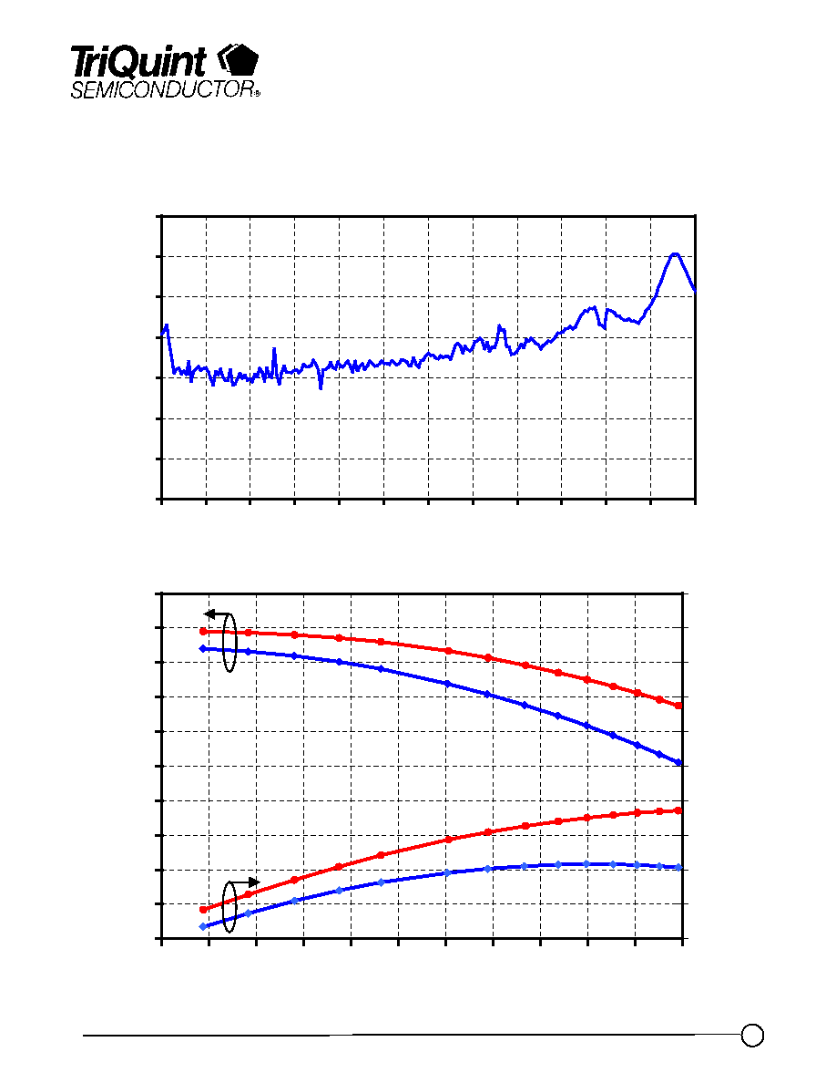
Measured Data
Bias Conditions: Vd = 6 V, Id = 50 mA
0
2
4
6
8
10
12
14
16
0
5
10
15
20
25
30
35
40
45
50
Frequency (GHz)
Output P1dB (dBm)
0
2
4
6
8
10
12
14
16
Noise Figure (dB)
NF at 4.5V,42 mA
P1dB at 4.5V,42 mA
P1dB at 6V,52 mA
0
2
4
6
8
10
12
14
16
18
0
10
20
30
40
50
60
70
80
Frequency (GHz)
Gain (dB)
-24
-20
-16
-12
-8
-4
0
Return Loss (dB)
Advance Product Information
June 30, 2005
5
TriQuint Semiconductor Texas Phone: (972)994 8465 Fax: (972)994 8504 Web: www.triquint.com Info:
info-mmw@tqs.com
TGA4811
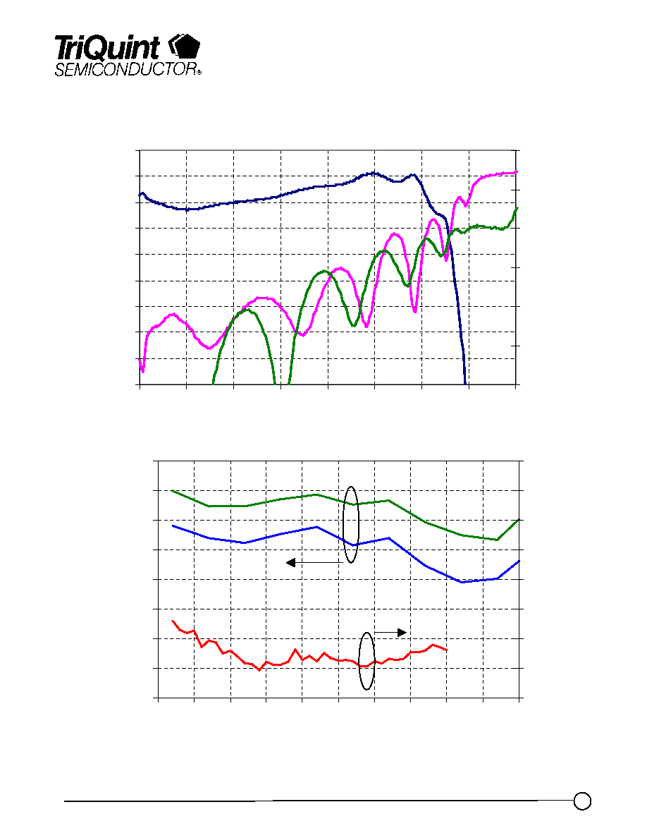
Measured Data
Bias Conditions: Vd = 6 V, Id = 50 mA
0
10
20
30
40
50
60
70
0
5
10
15
20
25
30
35
40
45
50
55
60
Frequency (GHz)
Group Del
ay (ps)
0
2
4
6
8
10
12
14
16
18
20
-11
-10
-9
-8
-7
-6
-5
-4
-3
-2
-1
0
Pin (dBm)
Gain
(d
B)
6
8
10
12
14
16
18
20
22
24
26
Ou
tp
u
t
Po
wer
(d
Bm)
6V, 52mA
6V, 52mA
4.5V, 42mA
4.5V, 42mA