TriQuint Semiconductor Texas Phone: (972)994-8465 Fax: (972)994 8504 Email: info-mmw@tqs.com Web: www.triquint.com
Advance Product Information
June 16, 2004
1
Note: Devices designated as EPU are typically early in their characterization process prior to finalizing all electrical and process
specifications. Specifications are subject to change without notice.
Wideband Low Noise Amplifier
TGA4830-EPU
Key Features and Performance
∑
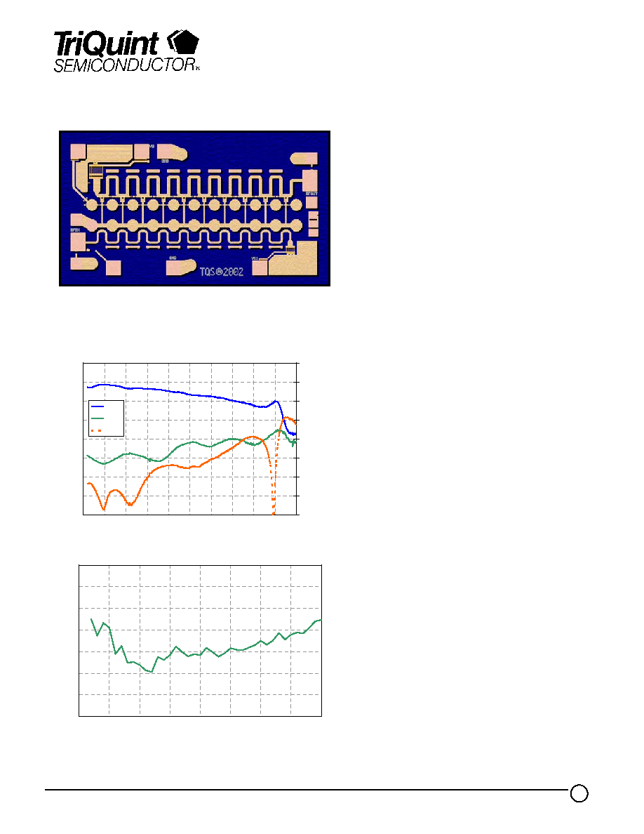
DC - 45GHz Frequency Range
∑
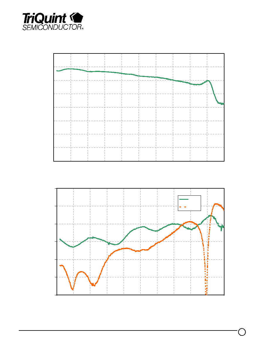
13dB Gain @ 20GHz
∑
15dB Return Loss @ 20GHz
∑
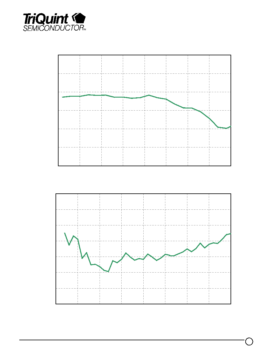
11.5dBm Typical P1dB
∑
3.2dB Typical Noise Figure
∑
40Gbps Data Rate
∑
> 20dB Gain Control
∑
0.15
µm pHEMT 3MI Technology
∑
5V, 50mA Bias Condition
∑
Chip Dimensions:
1.79 x 1.00 x 0.10 mm
(0.070 x 0.039 x 0.004 inches)
Primary Applications
∑
Test Equipment
∑
Ultra Wideband
∑
EW Systems
∑
Fiberoptic Systems
Measured Performance
V
+
= 5V, I
+
= 50mA
0
2
4
6
8
10
12
14
16
0
5
10
15
20
25
30
35
40
45
50
Frequency (GHz)
Gain (dB)
-30
-25
-20
-15
-10
-5
0
5
10
Return Loss (dB)
S21
S11
S22
Product Description
The TriQuint TGA4830-EPU is a medium power
wideband low noise amplifier which operates from DC
to 45 GHz. Typical small signal gain is 13dB with
>20dB AGC range. Typical input and output return loss
is 15dB. The TGA4830-EPU provides 11.5 dBm of
typical output power at 1 dB gain compression and a
3.2dB noise figure. RF ports are DC coupled enabling
the user to customize system corner frequencies.
The TGA4830-EPU is suitable for a variety of wideband
electronic warfare systems such as radar warning
receivers, electronic counter measures, decoys,
jammers and phased array systems. It is also an
excellent choice for 40Gb/s NRZ applications. The
TGA4830 is capable of driving an Electro-Absorptive
optical Modulator (EAM) with electrical Non-Return to
Zero (NRZ) data. In addition, the TGA4830 may also
be used as a predriver or a receive gain block.
0
1
2
3
4
5
6
7
0
5
10
15
20
25
30
35
40
Frequency (GHz)
Noise Figure (dB)

TriQuint Semiconductor Texas Phone: (972)994-8465 Fax: (972)994 8504 Email: info-mmw@tqs.com Web: www.triquint.com
Advance Product Information
June 16, 2004
2
Note: Devices designated as EPU are typically early in their characterization process prior to finalizing all electrical and process
specifications. Specifications are subject to change without notice.
TABLE I
MAXIMUM RATINGS
Symbol
Parameter 1/
Value
Notes
V
+
V
D
POSITIVE SUPPLY VOLTAGE
Biased Thru On-Chip Termination
Biased Thru RF Out
10 V
7 V
2/, 3/
I
+
I
D
POSITIVE SUPPLY CURRENT
Biased Thru On-Chip Termination
Biased Thru RF Out
72 mA
180m A
3/
P
D
+
P
D
POWER DISSIPATION
Biased Thru On-Chip Termination
Biased Thru RF Out
1.1 W
0.8 W
3/ 4/
V
G
Gate Voltage Range
-3V TO +1V
|I
G
|
Gate Current
10 mA
V
CTRL
Control Voltage Range
+5V TO
(V
D
≠ V
CTRL
8V)
5/
|I
CTRL
|
Control Current
10 mA
P
IN
Input Continuous Wave Power
TBD
V
IN
40Gbps PRBS Voltage Input
TBD
T
CH
Channel Temperature
150
∞C
6/
T
M
Mounting Temperature (30 Seconds)
320
0
C
T
STG
Storage Temperature
-65 to 150
0
C
1/ These ratings represent the maximum operable values for this device.
2/
Assure V
D
≠ V
CTRL
8V. Compute V
D
as follows: V
D
= V
+
- I
+
* 40
3/ Combinations of supply voltage, supply current, input power, and output power shall
not exceed P
D
.
4/ When operated at this bias condition with a base plate temperature of 70
0
C, the
median life is TBD hours.
5/
Assure V
CTRL
never exceeds V
D
during bias up and bias down sequences. Also,
V
CTRL
must never exceed 5V during normal operation.
6/
Junction operating temperature will directly affect the device mean time to failure
(MTTF). For maximum life it is recommended that junction temperatures be
maintained at the lowest possible levels
TGA4830-EPU

TriQuint Semiconductor Texas Phone: (972)994-8465 Fax: (972)994 8504 Email: info-mmw@tqs.com Web: www.triquint.com
Advance Product Information
June 16, 2004
3
Note: Devices designated as EPU are typically early in their characterization process prior to finalizing all electrical and process
specifications. Specifications are subject to change without notice.
TABLE III
RF CHARACTERIZATION TABLE
(T
A
= 25
∞C, Nominal)
(V
+
= 5V, I
+
= 50mA)
Symbol
Parameter
Test Conditions
Typ
Units Notes
Gain
Small Signal Gain
F = 1 ≠ 30 GHz
13
dB
BW
Small Signal 3dB
Bandwidth
45
GHz
IRL
Input Return Loss
F = 1 ≠ 30 GHz
12
dB
ORL
Output Return Loss
F = 1 ≠ 30 GHz
15
dB
P1dB
Output Power @ 1dB
Gain Compression
F = 1 ≠ 25 GHz
11.5
dBm
NF
Noise Figure
F = 1 ≠ 40 GHz
3.2
dB
Note: Table III Lists the RF Characteristics of typical devices as determined by fixtured
measurements.
TGA4830-EPU
TABLE II
THERMAL INFORMATION
Parameter
Test Conditions
T
CH
(
∞C)
R
JC
(
∞C/W)
MTTF
(hrs)
R
JC
Thermal Resistance
(Channel to Backside of
Carrier)
V
+
= 5V
I
+
= 50mA
P
DISS
= 0.25W
T
BASE
= 70
∞C
82.3
49.2
9.1E+8
Note: Assumes eutectic attach using 1.5mil 80/20 AuSn mounted to a 20mil CuMo
carrier at 70
∞C baseplate temperature. Worst case conditions with no RF applied,
100% of DC power is dissipated.

TriQuint Semiconductor Texas Phone: (972)994-8465 Fax: (972)994 8504 Email: info-mmw@tqs.com Web: www.triquint.com
Advance Product Information
June 16, 2004
4
Note: Devices designated as EPU are typically early in their characterization process prior to finalizing all electrical and process
specifications. Specifications are subject to change without notice.
Preliminary Data
V
+
= 5V, I
+
= 50mA
TGA4830-EPU
0
2
4
6
8
10
12
14
16
0
5
10
15
20
25
30
35
40
45
50
Frequency (GHz)
Gain (dB)
-30
-25
-20
-15
-10
-5
0
0
5
10
15
20
25
30
35
40
45
50
Frequency (GHz)
Return Loss (dB)
S11
S22

TriQuint Semiconductor Texas Phone: (972)994-8465 Fax: (972)994 8504 Email: info-mmw@tqs.com Web: www.triquint.com
Advance Product Information
June 16, 2004
5
Note: Devices designated as EPU are typically early in their characterization process prior to finalizing all electrical and process
specifications. Specifications are subject to change without notice.
TGA4830-EPU
Preliminary Data
V
+
= 5V, I
+
= 50mA
4
6
8
10
12
14
16
0
5
10
15
20
25
30
35
40
Frequency (GHz)
Pout @ P1dB (dBm)
0
1
2
3
4
5
6
7
0
5
10
15
20
25
30
35
40
Frequency (GHz)
Noise Figure (dB)
