Äîêóìåíòàöèÿ è îïèñàíèÿ www.docs.chipfind.ru

TriQuint Semiconductor Texas: (972)994 8465 Fax (972)994 8504 Email: info-mmw@tqs.com Web: www.triquint.com
Product Data Sheet
June 14, 2005
1
Note: Devices designated as EPU are typically early in their characterization process prior to finalizing all electrical and process
specifications. Specifications are subject to change without notice.
9.9-12.5Gb/s Optical Modulator Driver TGA8652-EPU-SL
OC-192 Metro and Long Haul Applications
Surface Mount Package
Key Features and Performance
·
DC - 12 GHz Linear BW
·
DC - 16 GHz Saturated Power BW
·
16 dB small signal gain
·
Wide Drive Range (4V to 8V)
·
25 ps Edge Rates (10/90)
·
Low Power Dissipation (1.4W at Vo=8V)
·
Package size: .350 x .350 x .084 inches.
·
Evaluation Board Available.
Primary Applications
·
Mach-Zehnder Modulator Driver
·
Pre-Driver
·
Receiver AGC
Description
The TriQuint TGA8652-EPU is a medium power wideband
AGC amplifier combined with off chip circuitry assembled in
a Surface Mount Package. The TGA8652-EPU typically
provides 16dB small signal gain with 6dB AGC range.
Typical input and output return loss is <10dB. Typical Noise
Figure is 2.5dB at 3GHz. Typical saturated output power is
25dBm. Small signal 3dB BW is 12GHz with saturated
power performance to 16GHz. RF ports are DC coupled
enabling the user to customize system corner frequencies.
Applications include OC192 12.5GBit/s NRZ MZ Modulator
Driver and receive AGC amplifier.
Drain bias may be applied thru the on-chip drain termination
resistor for low drive applications or thru the RF output port
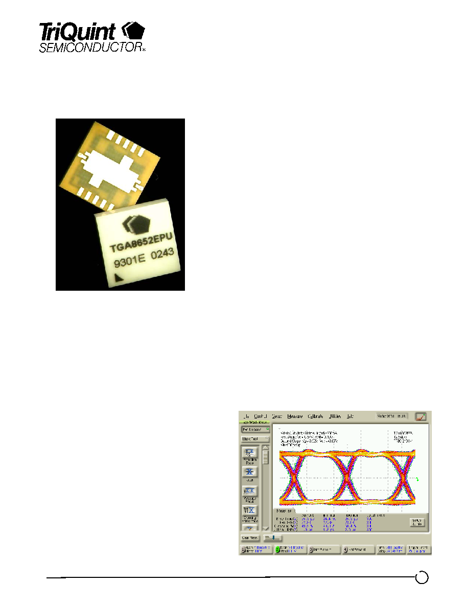
for high drive applications. A cascaded pair demonstrated
8Vpp output voltage swing with 500mVpp at the input when
stimulated with 10GBit/s. 2^31-1prbs. NRZ data.
The TGA8652-EPU is available on an evaluation board.
Cascaded 8652 Evaluation Boards
12.5 Gb/s Performance
Output = 8 Vpp, Input = 500 mVpp
Scale: 2 V/div, 20 ps/div
Measured Performance

TriQuint Semiconductor Texas: (972)994 8465 Fax (972)994 8504 Email: info-mmw@tqs.com Web: www.triquint.com
Product Data Sheet
June 14, 2005
2
Note: Devices designated as EPU are typically early in their characterization process prior to finalizing all electrical and process
specifications. Specifications are subject to change without notice.
SYMBOL
PARAMETER 1/
VALUE
NOTES
V
+
Vd(RFout)
POSITIVE SUPPLY VOLTAGE
Drain bias applied thru on-chip termination
Drain bias applied at RF output using bias T
12 V
10 V
V
+
Id
POSITIVE SUPPLY CURRENT
Drain bias applied thru on-chip termination
Drain bias applied at RF output using bias T
110 mA
250 mA
2/
P
d
POWER DISSIPATION
2.4 W
3/
Vg
Ig
NEGATIVE GATE
Voltage
Gate Current
0 V to 3 V
5 mA
Vctrl
Ictrl
CONTROL GATE
Voltage
Gate Current
Vd/2 to 3 V
5 mA
4/
P
IN
RF INPUT
Sinusoidal Continuous Wave Power
23 dBm
T
CH
OPERATING CHANNEL TEMPERATURE
150
0
C
5/ 6/
T
STG
STORAGE TEMPERATURE
-40 to 125
0
C
Notes:
1/ These ratings represent the maximum operable values for the device.
2/ Assure the combination of Vd and Id does not exceed maximum power dissipation rating.
3/ When operated at this bias condition with a base plate temperature of 80
0
C, the Mean Time to Failure
(MTTF) is reduced from 2.6E+7 to 1E+6 hours.
4/ Assure Vctrl never exceeds Vd during bias on and off sequences, and normal operation.
5/ These ratings apply to each individual FET.
6/ Junction operating temperature will directly affect the device median time to failure (MTTF). For maximum
life, it is recommended that junction temperatures be maintained at the lowest possible levels.
MAXIMUM RATINGS

TriQuint Semiconductor Texas: (972)994 8465 Fax (972)994 8504 Email: info-mmw@tqs.com Web: www.triquint.com
Product Data Sheet
June 14, 2005
3
Note: Devices designated as EPU are typically early in their characterization process prior to finalizing all electrical and process
specifications. Specifications are subject to change without notice.
THERMAL INFORMATION*
Parameter
Test Condition
T
CH
(
°C)
R
JC
(
°C/W)
MTTF
(HRS)
R
JC
Thermal Resistance
(channel to backside of package)
Vd(RF out) = 6.5 V, Vctrl = 1 V,
Id = 170 mA
± 5%,
T
base
= 80
°C
114.70
31.40
2.6E+7
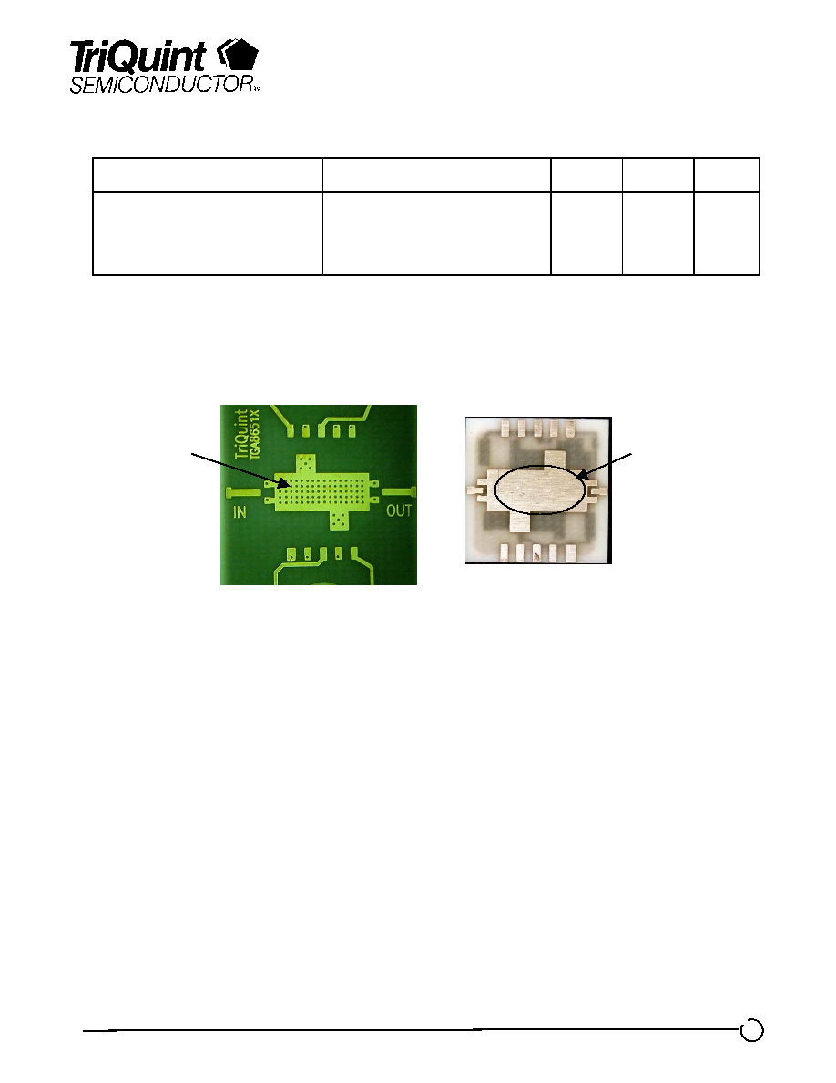
NOTE: Thermal transfer is conducted thru the bottom of the TGA8652-EPU package into the
motherboard. Design the motherboard to assure adequate thermal transfer to the base plate. An array
of filled thermal vias is recommended as shown in the example below.
* This information is a result of a thermal model.
Thermal vias
in motherboard
Area of thermal
transfer
Bottom View TGA8652-EPU
Motherboard

TriQuint Semiconductor Texas: (972)994 8465 Fax (972)994 8504 Email: info-mmw@tqs.com Web: www.triquint.com
Product Data Sheet
June 14, 2005
4
Note: Devices designated as EPU are typically early in their characterization process prior to finalizing all electrical and process
specifications. Specifications are subject to change without notice.
RF SPECIFICATIONS
(T
A
= 25
°C Nominal)
VALUE
NOTE
TEST
MEASUREMENT
CONDITIONS
MIN
TYP
MAX
UNITS
SMALL SIGNAL BW
12
GHz
SATURATED POWER BW
16
GHz
1/, 2/
SMALL-SIGNAL
GAIN MAGNITUDE
2 and 4 GHz
6 GHz
10 GHz
14 GHz
16 GHz
15
13
13
10
10
16
15
14
13
13
dB
SMALL SIGNAL AGC RANGE
Midband
15
dB
1/, 2/
INPUT RETURN LOSS
MAGNITUDE
2, 4, 6, and 10 GHz
14 and 18 GHz
9
8
10
10
dB
1/, 2/
OUTPUT RETURN LOSS
MAGNITUDE
2, 4, 6, and 10 GHz
14 and 18 GHz
10
8
10
10
dB
6/, 7/
SATURATED OUTPUT
POWER
2, 4, 6, 8, and
10 GHz
25
dBm
3/, 4/
EYE AMPLITUDE
Vd (RFout) = 7 V
Vd (RFout) = 6 V
Vd (RFout) = 5 V
Vd (RFout) = 4.5 V
8.0
7.0
6.0
5.5
Vpp
3/, 4/, 5/ ADDITIVE JITTER (p-p)
5
ps
3/, 4/
RISE TIME (10/90)
25
ps
Notes:
1/ Verified at package level RF probe.
2/ Package Probe Bias: V
+
= 8 V, adjust Vg1 to achieve Id = 87 mA, Vctrl = +1 V
3/ Verified by design, TGA8652EPU assembled onto a demonstration board shown on page 7 then tested
using the application circuit and bias procedure detailed on pages 8 and 9.
4/ Vin = 2 V, Data Rate = 12.5 Gb/s, Vctrl and Vg are adjusted for maximum output.
5/ Computed using RSS Method where Jpp_additive = SQRT(Jpp_out
2
- Jpp_in
2
)
6/ Verified at die level on-wafer probe.
7/ Power Bias Die Probe: VDT=8 V, adjust Vg to achieve Id = 175 mA+/-5%, Vctrl = 1.5 V
Note: At the die level, drain bias is applied thru the RF output port using a bias tee, voltage
is at the DC input to the bias tee.

TriQuint Semiconductor Texas: (972)994 8465 Fax (972)994 8504 Email: info-mmw@tqs.com Web: www.triquint.com
Product Data Sheet
June 14, 2005
5
Note: Devices designated as EPU are typically early in their characterization process prior to finalizing all electrical and process
specifications. Specifications are subject to change without notice.
-35
-30
-25
-20
-15
-10
-5
0
0
1
2
3
4
5
6
7
8
9
10 11 12 13 14 15
16
Frequency (GHz)
R
e
t
u
r
n
Los
s
(
d
B
)
0
2
4
6
8
10
12
14
16
18
20
0
1
2
3
4
5
6
7
8
9
10
11 12 13 14 15
16
Frequency (GHz)
Ga
in
(
d
B
)
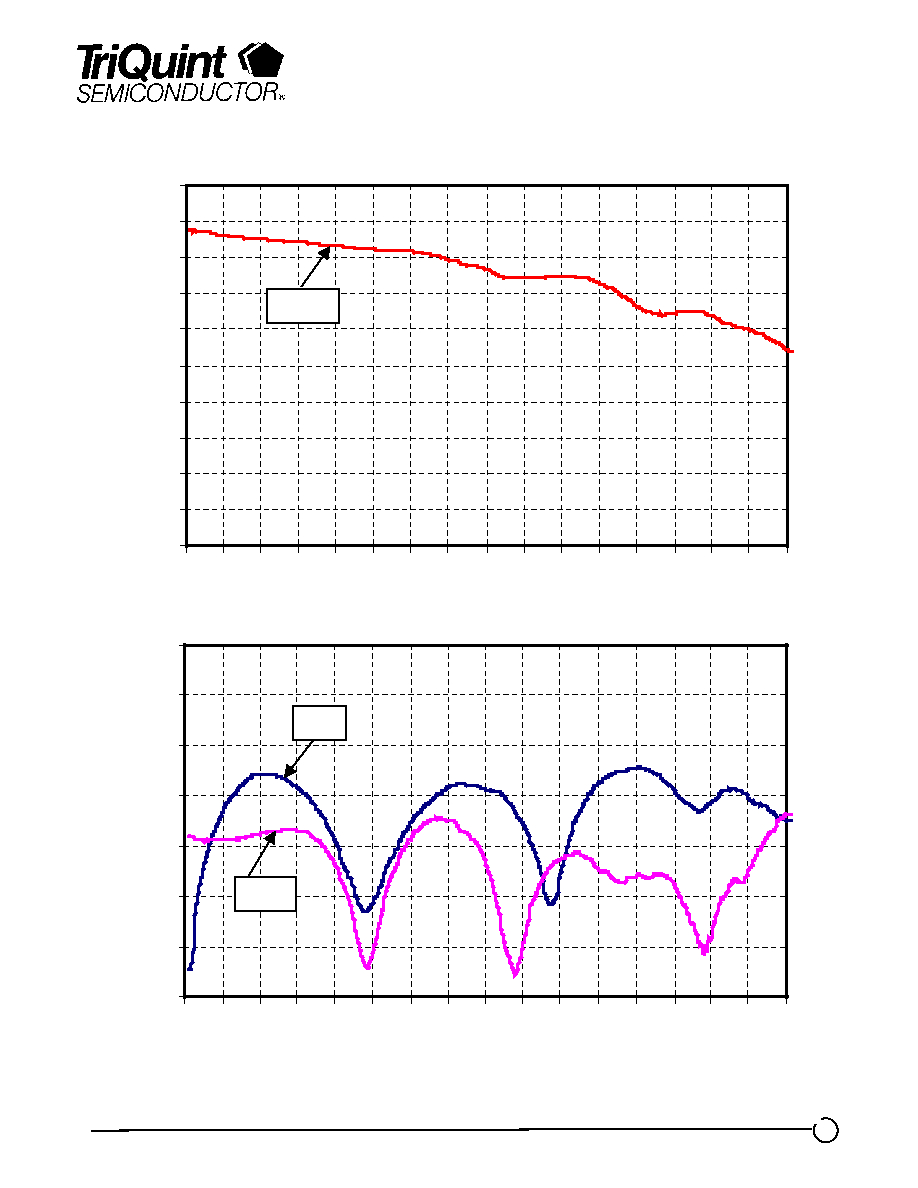
Typical Measured S-parameters
IRL
ORL
GAIN
Document Outline
