TriQuint Semiconductor Texas : Phone (972)994-8465 Fax (972)994 8504 Web: www.triquint.com
Product Datasheet
1
rev 11/10/98
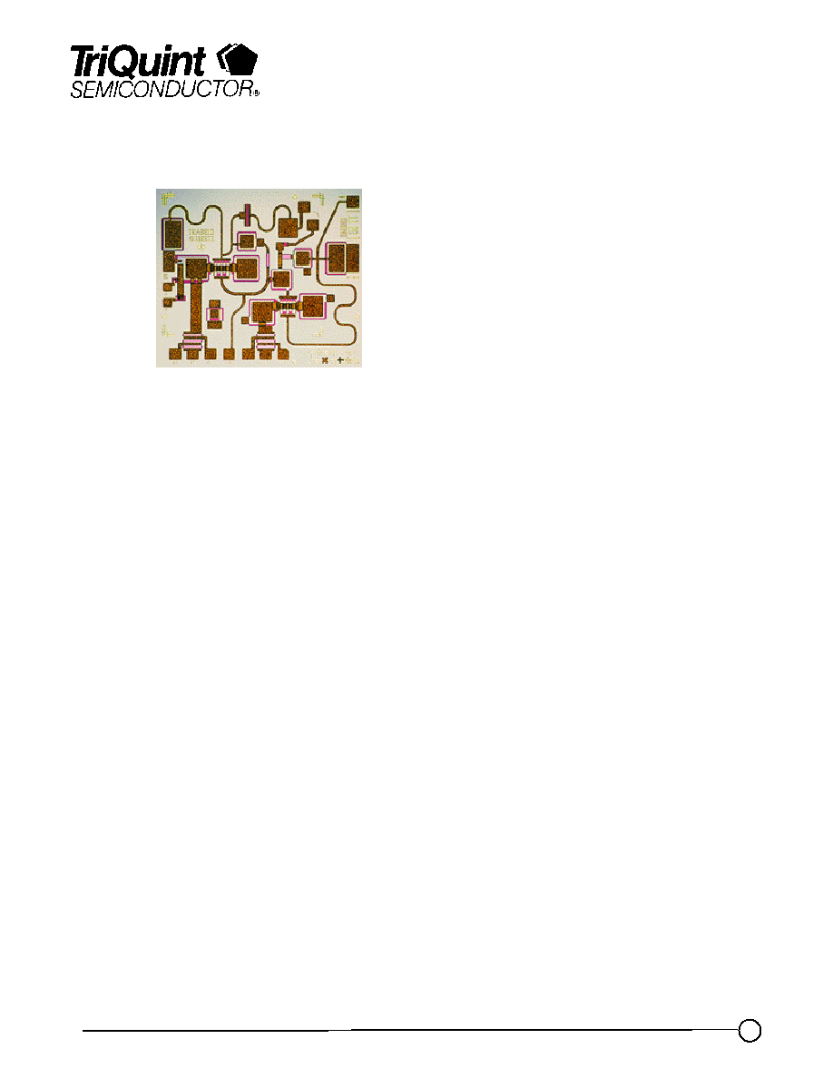
2-10 GHz Gain Block Amplifier TGA8810-SCC
Key Features and Performance
∑
2 to 10-GHz Frequency Range
∑
Operates from Single 5-V Supply
∑
Unconditionally Stable
∑
17-dB Typical Gain
∑
Typical ± 0.6-dB Gain Flatness
∑
1,8796 x 1,6510 x 0,1524 mm
(0.074 x 0.065 x 0.006 in.)
The TriQuint TGA8810-SCC is a self-biased general purpose amplifier. Two gain stages employ shunt
feedback to produce flat gain to 10-GHz. Output power at 1-dB gain compression is typically 17-dBm and
noise figure is 6-dB. The TGA8810-SCC uses on-chip DC blocks to allow direct cascading. Three different
on-chip self-bias resistors provide the flexibility of selecting bias current and RF performance.
The TGA8810-SCC is available in chip form and is readily assembled using automated equipment.
Bond pad and backside metallization is gold plated for compatibility with eutectic alloy attachment methods
as well as the thermocompression and thermosonic wire-bonding processes.
November 13, 2001
TriQuint Semiconductor Texas : Phone (972)994-8465 Fax (972)994 8504 Web: www.triquint.com
Product Datasheet
2
rev 11/10/98
TGA8810-SCC
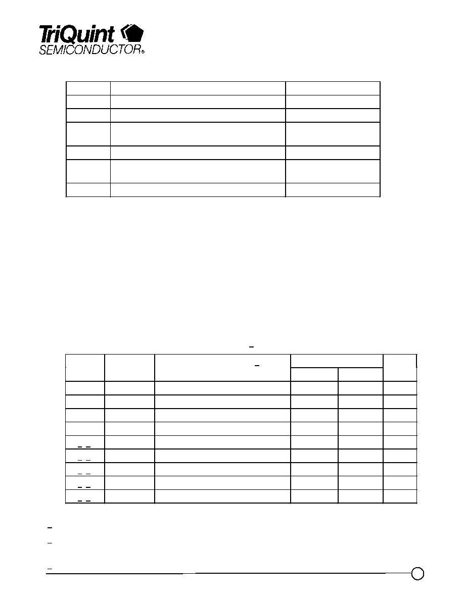
TABLE I
MAXIMUM RATINGS
SYMBOL
PARAMETER
VALUE
V
+
POSITIVE SUPPLY VOLTAGE V
D1
, V
D2
8.5 V
I
-
NEGATIVE SUPPLY CURRENT
-2.91mA
P
D
POWER DISSIPATION AT (OR BELOW) 25
∞
C
BASE-PLATE TEMPERATURE
*
2.4 W
T
CH
**
OPERATING CHANNEL TEMPERATURE
150
0
C
T
M
MOUNTING TEMPERATURE
(30 SECONDS)
320
0
C
T
STG
STORAGE TEMPERATURE
-65 to 150
0
C
Ratings over channel temperature range, T
CH
(unless otherwise noted)
Stresses beyond those listed under "Maximum Ratings" may cause permanent damage to the
device.
These are stress ratings only, and functional operation of the device at these or any other
conditions beyond those indicated under "RF Characteristics" is not implied. Exposure to
maximum rated conditions for extended periods may affect device reliability.
*For operation above 25
∞
C base-plate temperature, derate linearly at the rate of 5mW/
∞
C.
** Operating channel temperature, T
CH
, directly affects the device MTTF. For maximum life, it is
recommended that channel temperature be maintained at the lowest possible level.
TABLE II
DC SPECIFICATIONS (100%)
(T
A
= 25
∞
C + 5
∞
C)
NOTES
SYMBOL
TEST CONDITIONS 2/
LIMITS
UNITS
MIN
MAX
I
DSS1
STD
50
150
mA
I
DSS2
STD
50
150
mA
G
M1
STD
70
140
mS
G
M2
STD
70
140
mS
1/,3/
|V
P1
|
STD
0.5
2.3
V
1/,3/
|V
P2
|
STD
0.5
2.3
V
1/,3/
|V
BVGD1
|
STD
6
30
V
1/,3/
|V
BVGD2
|
STD
6
30
V
1/,3/
|V
BVGS1
|
STD
6
30
V
1/
V
P
, V
BVGD
, and V
BVGS
are negative.
2/
The measurement conditions are subject to change at the manufacture's discretion (with appropriate
notification to the buyer).
3/
STD refers to Standard Test Conditions, see Table IV.
TriQuint Semiconductor Texas : Phone (972)994-8465 Fax (972)994 8504 Web: www.triquint.com
Product Datasheet
3
rev 11/10/98
TGA8810-SCC
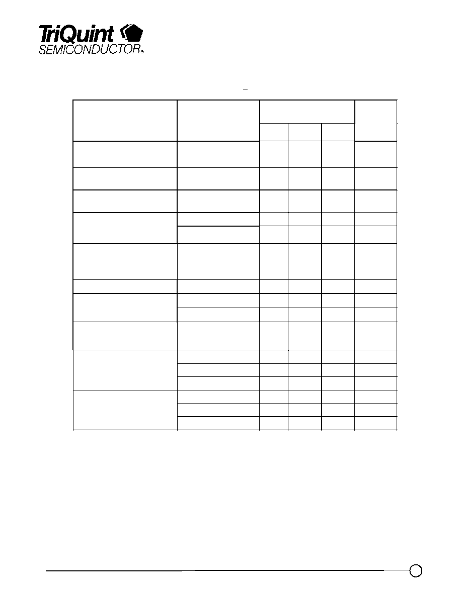
TABLE III
RF SPECIFICATIONS
(T
A
= 25
∞
C + 5
∞
C)
TEST
MEASUREMENT
CONDITIONS
VALUE
UNITS
V
+
= 5V, I
+
= 60mA
Self Bias
MIN
TYP
MAX
SMALL-SIGNAL
GAIN MAGNITUDE
F = 2 ≠ 10 GHz
14
17
dB
INPUT STANDING WAVE
RATIO
F = 2 ≠ 10 GHz
1.9:1
OUTPUT STANDING WAVE
RATIO
F = 2 ≠ 10 GHz
1.2:1
F = 2 ≠ 10 GHz
±
0.6
3.0
dB
SMALL-SIGNAL GAIN
RIPPLE
F = 2 GHz
-0.01
dB
POWER OUTPUT
AT 1 dB GAIN
COMPRESSION
F = 2 ≠ 10 GHz
13
17
dBm
NOISE FIGURE
F = 2 ≠ 10 GHz
6
7.5
dB
F = 2 ≠ 9.5 GHz
8
dB
INPUT RETURN LOSS
MAGNITUDE
F = 9.5 ≠ 10 GHz
4
dB
OUTPUT RETURN LOSS
MAGNITUDE
F = 2 ≠ 10 GHz
9
dB
F = 2 GHz
24
dBm
F = 5 GHz
26
dBm
OUTPUT THIRD ORDER
INTERCEPT
F = 8 GHz
25
dBm
F = 2 GHz
-0.01
dB/
∞
C
F = 6 GHz
-0.02
dB/
∞
C
GAIN TEMPERATURE
COEFFICIENT
(T
BP
= -40
∞
C to 90
∞
C)
F = 10 GHz
-0.02
dB/
∞
C
TriQuint Semiconductor Texas : Phone (972)994-8465 Fax (972)994 8504 Web: www.triquint.com
Product Datasheet
4
rev 11/10/98
TABLE IV
AUTOPROBE FET PARAMETER MEASUREMENT CONDITONS
FET Parameters
Test Conditions
I
DSS
: Maximum drain current (I
DS
) with gate voltage
(V
GS
) at zero volts.
V
GS
= 0.0 V, drain voltage (V
DS
) is swept from 0.5 V
up to a maximum of 3.5 V in search of the maximum
value of I
DS
; voltage for I
DSS
is recorded as VDSP.
G
m
: Transconductance;
I
DSS
-
IDS 1
(
)
VG1
For all material types, V
DS
is swept between 0.5 V
and VDSP in search of the maximum value of I
ds
.
This maximum I
DS
is recorded as IDS1. For
Intermediate and Power material, IDS1 is measured
at V
GS
= VG1 = -0.5 V. For Low Noise, HFET and
pHEMT material, V
GS
= VG1 = -0.25 V. For
LNBECOLC, use V
GS
= VG1 = -0.10 V.
V
P
: Pinch-Off Voltage; V
GS
for I
DS
= 0.5 mA/mm of
gate width.
V
DS
fixed at 2.0 V, V
GS
is swept to bring I
DS
to
0.5 mA/mm.
V
BVGD
: Breakdown Voltage, Gate-to-Drain; gate-to-
drain breakdown current (I
BD
) = 1.0 mA/mm
of gate width.
Drain fixed at ground, source not connected
(floating), 1.0 mA/mm forced into gate, gate-to-drain
voltage (V
GD
) measured is V
BVGD
and recorded as
BVGD; this cannot be measured if there are other
DC connections between gate-drain, gate-source or
drain-source.
V
BVGS
: Breakdown Voltage, Gate-to-Source; gate-to-
source breakdown current (I
BS
) = 1.0 mA/mm
of gate width.
Source fixed at ground, drain not connected
(floating), 1.0 mA/mm forced into gate, gate-to-
source voltage (V
GS
) measured is V
BVGS
and recorded
as BVGS; this cannot be measured if there are other
DC connections between gate-drain, gate-source or
drain-source.
TGA8810-SCC
TriQuint Semiconductor Texas : Phone (972)994-8465 Fax (972)994 8504 Web: www.triquint.com
Product Datasheet
5
rev 11/10/98
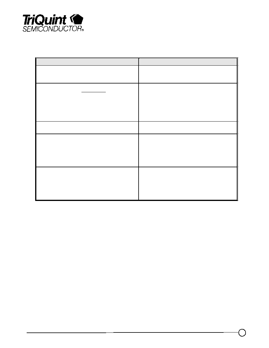
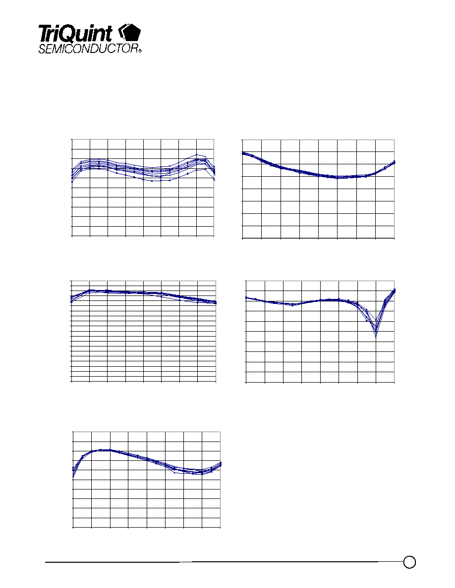
TGA8810 - Fixture Data Summary
V+=5V, Self Biased, Ta=25C
s21
P1dB
s11
TGA8810-SCC
10
11
12
13
14
15
16
17
18
19
20
2.0
3.0
4.0
5.0
6.0
7.0
8.0
9.0
10.0
Frequency (GHz)
Ga
in
(
d
B
)
0
1
2
3
4
5
6
7
8
2.0
3.0
4.0
5.0
6.0
7.0
8.0
9.0
10.0
Frequency (GHz)
Noi
s
e
Fi
gur
e
(
d
B)
Noise Figure
0
1
2
3
4
5
6
7
8
9
10
11
12
13
14
15
16
17
18
19
20
2
3
4
5
6
7
8
9
10
Frequency (GHz)
Pout @1dB Compression (dBm)
-50
-45
-40
-35
-30
-25
-20
-15
-10
-5
0
2.0
3.0
4.0
5.0
6.0
7.0
8.0
9.0
10.0
Frequency (GHz)
Input Return Loss (dB)
-50
-45
-40
-35
-30
-25
-20
-15
-10
-5
0
2.0
3.0
4.0
5.0
6.0
7.0
8.0
9.0
10.0
Frequency (GHz )
O
u
t
put
R
e
t
u
r
n
Loss (
d
B
)
s22