1
TriQuint Semiconductor Texas: Phone (972)994 8465 Fax (972)994 8504 Web: www.triquint.com/mmw
Product Data Sheet
January 10, 2005
6 - 18 GHz High Power Amplifier TGA9092-SCC
Key Features and Performance
∑
Dual Channel Power Amplifier
∑
0.25um pHEMT Technology
∑
6-18 GHz Frequency Range
∑
2.8 W/Channel Midband Pout
∑
5.6 W Pout Combined
∑
24 dB Nominal Gain
∑
Balanced In/Out for Low VSWR
∑
8V @ 1.2A per Channel Bias
Primary Applications
∑
X-Ku band High Power
∑
VSAT
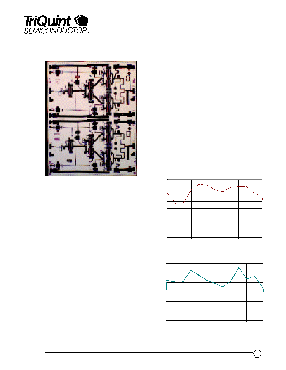
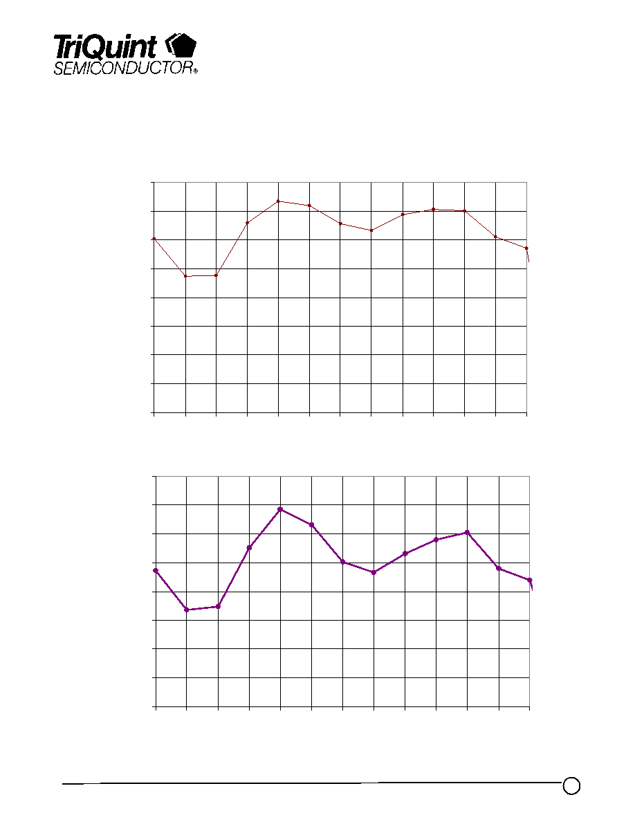
Typical Measured Small Signal Gain
Typical Measured Pout (RF Probe)
Product Description
The TriQuint TGA9092-SCC is a dual channel, three-
stage wide band HPA MMIC designed using TriQuint's
proven 0.25
µ
m Power pHEMT process to support a
variety of high performance applications including
military EW programs, VSAT, and other applications
requiring wideband high power performance.
Each amplifier channel consists of one 1200
µ
m input
device driving a 2400
µ
m intermediate stage which
drives a 4800 um output stage.
The TGA9092-SCC provides a nominal 34 dBm of
output power at 2dB gain compression across the 6-18
GHz range per channel . Power combined, nominal
output power of 36.5 dBm can be expected with low
loss external couplers. Typical per channel small
signal gain is 24 dB. Typical single-ended Input/Output
RL is 6-8 dB across the band.
The TGA9092-SCC is 100% DC and RF tested on-
wafer to ensure performance compliance. The device
is available in chip form.
15
16
17
18
19
20
21
22
23
24
25
26
27
6
7
8
9
10
11
12
13
14
15
16
17
18
Frequency (GHz)
G
a
in
(
d
B
)
Chip Dimensions 5.739 mm x 4.318 mm x 0.1016 mm
28
29
30
31
32
33
34
35
36
6
7
8
9
10
11
12
13
14
15
16
17
18
Frequency (GHz)
Po
u
t
@ P2d
B
(
d
B
m
)

2
TriQuint Semiconductor Texas: Phone (972)994 8465 Fax (972)994 8504 Web: www.triquint.com/mmw
Product Data Sheet
January 10, 2005
TABLE I
MAXIMUM RATINGS
Symbol
Parameter 5/
Value
Notes
V
+
Positive Supply Voltage
9 V
4/
V
-
Negative Supply Voltage Range
-5V TO 0V
I
+
Positive Supply Current (Quiescent)
3.5 A
4/
| I
G
|
Gate Supply Current
84.48 mA
P
IN
Input Continuous Wave Power
26 dBm
4/
P
D
Power Dissipation
28.8 W
3/ 4/
T
CH
Operating Channel Temperature
150
0
C
1/ 2/
T
M
Mounting Temperature
(30 Seconds)
320
0
C
T
STG
Storage Temperature
-65 to 150
0
C
1/
These ratings apply to each individual FET.
2/
Junction operating temperature will directly affect the device median time to failure (T
M
).
For maximum life, it is recommended that junction temperatures be maintained at the
lowest possible levels.
3/
When operated at this bias condition with a base plate temperature of 70
0
C, the median
life is reduced from 1.6 E+6 to 5.4 E+4 hours.
4/
Combinations of supply voltage, supply current, input power, and output power shall not
exceed P
D
.
5/
These ratings represent the maximum operable values for this two-channel device.
TGA9092-SCC

3
TriQuint Semiconductor Texas: Phone (972)994 8465 Fax (972)994 8504 Web: www.triquint.com/mmw
Product Data Sheet
January 10, 2005
TGA9092-SCC
TABLE II
DC PROBE TEST
(TA = 25
∞
C
±
5
∞
C)
Symbol
Parameter
Minimum
Maximum
Unit
Imax
(Q1)
Maximum Current
400
800
mA
Gm
(Q1)
Transconductance
200
600
mS
V
P
Pinch-off Voltage
-1.5
-0.5
V
BVGS
Breakdown Voltage Gate-
Source
-30
-13
V
BVGD
Breakdown Voltage Gate-
Drain
-30
-13
V
TABLE III
AUTOPROBE FET PARAMETER MEASUREMENT CONDITONS
FET Parameters
Test Conditions
G
m
: Transconductance;
I
DSS
-
IDS 1
(
)
VG1
For all material types, V
DS
is swept between 0.5 V
and VDSP in search of the maximum value of I
ds
.
This maximum I
DS
is recorded as IDS1. For
Intermediate and Power material, IDS1 is measured
at V
GS
= VG1 = -0.5 V. For Low Noise, HFET and
pHEMT material, V
G S
= VG1 = -0.25 V. For
LNBECOLC, use V
G S
= VG1 = -0.10 V.
V
P
: Pinch-Off Voltage; V
GS
for I
DS
= 0.5 mA/mm of
gate width.
V
DS
fixed at 2.0 V, V
GS
is swept to bring I
DS
to
0.5 mA/mm.
V
BVGD
: Breakdown Voltage, Gate-to-Drain; gate-to-
drain breakdown current (I
BD
) = 1.0 mA/mm
of gate width.
Drain fixed at ground, source not connected
(floating), 1.0 mA/mm forced into gate, gate-to-drain
voltage (V
GD
) measured is V
BDGD
and recorded as
BVGD; this cannot be measured if there are other
DC connections between gate-drain, gate-source or
drain-source.
V
BVGS
: Breakdown Voltage, Gate-to-Source; gate-to-
source breakdown current (I
BS
) = 1.0 mA/mm
of gate width.
Source fixed at ground, drain not connected
(floating), 1.0 mA/mm forced into gate, gate-to-
source voltage (V
GS
) measured is V
BDGS
and recorded
as BVGS; this cannot be measured if there are other
DC connections between gate-drain, gate-source or
drain-source.
I
MAX
: Maximum I
D S
.
Positive voltage is applied to the gate to saturate the
device. V
DS
is stepped between 0.5 V up to a
maximum of 3.5 V, searching for the maximum
value of I
DS
.

4
TriQuint Semiconductor Texas: Phone (972)994 8465 Fax (972)994 8504 Web: www.triquint.com/mmw
Product Data Sheet
January 10, 2005
TABLE V
THERMAL INFORMATION*
Parameter
Test Conditions
T
CH
(
o
C)
R
JC
(
∞
C/W)
T
M
(HRS)
R
JC
Thermal Resistance
(channel to backside of
carrier)
Vd = 8 V
I
D
= 2.4 A
Pdiss = 19.2 W
144.56
3.88
1.6 E+6
Note: Assumes eutectic attach using 1.5 mil 80/20 AuSn mounted to a 20 mil CuMo Carrier
at 70
∞
C baseplate temperature. Worst case condition with no RF applied, 100% of DC
power is dissipated.
* This information is a result of a thermal model analysis based on the entire two-channel
device.
TGA9092-SCC
TABLE IV
RF WAFER CHARACTERIZATION TEST*
(T
A
= 25
∞
C + 5
∞
C)
(Vd = 8V, Id = 1.2A
±
5%)
Parameter
Test Condition
Limit
Min Nom Max
Units
Small-signal
Power Gain
F = 6 to 17 GHz
F = 18 GHz
20
18
24
-
dB
Input Return
Loss
F = 6 to 18 GHz
6
dB
Output Return
Loss
F = 6 to 18 GHz
8
dB
Output Power
@ 2dB gain
compression
F = 6 to 8 GHz
F = 9 to 18 GHz
32
32.5
34.5
-
-
dBm
Power Added
Efficiency
F = 6 to 18 GHz
12
25
-
%
Note: RF probe data taken at 1 GHz steps
* This information is based on the per-channel device.

5
TriQuint Semiconductor Texas: Phone (972)994 8465 Fax (972)994 8504 Web: www.triquint.com/mmw
Product Data Sheet
January 10, 2005
Data Based on the 50th Percentile On-Wafer RF
Probe Test Results, Sample Size = 3370 Devices
Bias Conditions: Vd = 8 V, Id = 1.2 A
TGA9092-SCC
0
5
10
15
20
25
30
35
40
6
7
8
9
10
11
12
13
14
15
16
17
18
Frequency (GHz)
PA
E (%
)
28
29
30
31
32
33
34
35
36
6
7
8
9
10
11
12
13
14
15
16
17
18
Frequency (GHz)
P
out
@
P
2
dB
(
dB
m
)


