Advance Product Information
September 19, 2005
TriQuint Semiconductor Texas: Phone (972)994-8465 Fax (972)994-8504 Email: Info-mmw@tqs.com Web: www.triquint.com
1
0
5
10
15
20
25
30
35
0
2
4
6
8
10
12
14
16
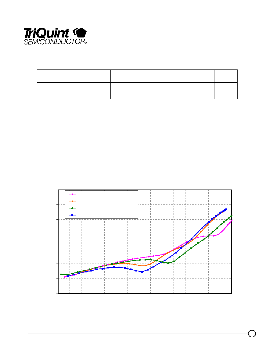
Frequency (GHz)
Maximum Gain (dB
)
MAG
MSG
DC - 20 GHz Discrete power pHEMT TGF2022-06
Key Features and Performance
�
Frequency Range: DC - 20 GHz
�
> 28 dBm Nominal Psat
�
58% Maximum PAE
�
36 dBm Nominal OIP3
�
13 dB Nominal Power Gain
�
Suitable for high reliability applications
�
0.6mm x 0.35 m Power pHEMT
�
Nominal Bias Vd = 8-12V, Idq = 45-75mA
(U
nder RF Drive, Id rises from 45mA to 150mA)
�
Chip Dimensions: 0.57 x 0.53 x 0.10 mm
(0.022 x 0.021 x 0.004 in)
Primary Applications
�
Point-to-point Radio
�
High-reliability space
�
Military
�
Base Stations
�
Broadband Wireless Applications
Product Description
The TriQuint TGF2022-06 is a discrete
0.6 mm pHEMT which operates from
DC-20 GHz. The TGF2022-06 is
designed using TriQuint's proven
standard 0.35um power pHEMT
production process.
The TGF2022-06 typically provides
> 28 dBm of saturated output power with
power gain of 13 dB. The maximum
power added efficiency is 58% which
makes the TGF2022-06 appropriate for
high efficiency applications.
The TGF2022-06 is also ideally suited for
Point-to-point Radio, High-reliability
space, and Military applications.
The TGF2022-06 has a protective
surface passivation layer providing
environmental robustness.
Lead-free and RoHS compliant
Note: This device is early in the characterization process prior to finalizing all electrical specifications. Specifications are subject to
change without notice.

Advance Product Information
September 19, 2005
TriQuint Semiconductor Texas: Phone (972)994-8465 Fax (972)994-8504 Email: Info-mmw@tqs.com Web: www.triquint.com
2
TABLE I
MAXIMUM RATINGS
Symbol
Parameter 1/
Value
Notes
V
+
Positive Supply Voltage
12.5 V
2/
V
-
Negative Supply Voltage Range
-5V to 0V
I
+
Positive Supply Current
282 mA
2/
| I
G
|
Gate Supply Current
7 mA
P
IN
Input Continuous Wave Power
23 dBm
2/
P
D
Power Dissipation
See note 3
2/ 3/
T
CH
Operating Channel Temperature
150
�
C
4/
T
M
Mounting Temperature (30 Seconds)
320
�
C
T
STG
Storage Temperature
-65 to 150
�
C
1/
These ratings represent the maximum operable values for this device.
2/
Combinations of supply voltage, supply current, input power, and output power shall
not exceed P
D
.
3/
For a median life time of 1E+6 hrs, Power dissipation is limited to:
P
D
(max) = (150
�
C � TBASE
�
C) / 138.0 (
�
C/W)
4/
Junction operating temperature will directly affect the device median time to failure
(T
M
). For maximum life, it is recommended that junction temperatures be maintained
at the lowest possible levels.
TGF2022-06
TABLE II
DC PROBE CHARACTERISTICS
(T
A
= 25
q
C, Nominal)
Symbol
Parameter
Minimum
Typical
Maximum
Unit
Idss
Saturated Drain Current
-
180
-
mA
Gm
Transconductance
-
225
-
mS
V
P
Pinch-off Voltage
-1.5
-1
-0.5
V
V
BGS
Breakdown Voltage
Gate-Source
-30
-
-14
V
V
BGD
Breakdown Voltage
Gate-Drain
-30
-
-14
V
Note: For TriQuint's 0.35um power pHEMT devices, RF breakdown >> DC breakdown

Advance Product Information
September 19, 2005
TriQuint Semiconductor Texas: Phone (972)994-8465 Fax (972)994-8504 Email: Info-mmw@tqs.com Web: www.triquint.com
3
TABLE III
RF CHARACTERIZATION TABLE
(T
A
= 25
�
C, Nominal)
SYMBOL
PARAMETER
f = 10 GHz
f = 18 GHz
UNITS
Vd = 10V
Idq = 45 mA
Vd = 12V
Idq = 45 mA
Vd = 10V
Idq = 45 mA
Vd = 12V
Idq = 45 mA
Power Tuned:
Psat
PAE
Gain
Rp 1/
Cp 1/
L
2/
Saturated Output Power
Power Added Efficiency
Power Gain
Parallel Resistance
Parallel Capacitance
Load Reflection
coefficient
28.9
52.4
12.9
44.63
0.276
0.382
120.1
29.6
51.9
12.9
56.99
0.257
0.400
104.7
28.1
41.5
8.3
43.55
0.415
0.522
127.7
28.7
37.0
8.0
48.44
0.432
0.556
125.1
dBm
%
dB
pF
-
Efficiency
Tuned:
Psat
PAE
Gain
Rp 1/
Cp 1/
L
2/
Saturated Output Power
Power Added Efficiency
Power Gain
Parallel Resistance
Parallel Capacitance
Load Reflection
coefficient
28.3
58.3
13
72.49
0.252
0.455
93.7
29.3
56.0
13
74.22
0.255
0.466
93.4
27.5
46.0
8.5
51.30
0.495
0.619
127.3
28.1
42.5
8.3
66.97
0.503
0.680
123.0
dBm
%
dB
pF
-
OIP3
Output TOI
37
36
37
36
dBm
TGF2022-06
1/ Large signal equivalent pHEMT output network
2/ Optimum load impedance for maximum power or maximum PAE at 10 and 18 GHz. The series
resistance and inductance (Rd and Ld) shown in the Figure on page 7 is excluded

Advance Product Information
September 19, 2005
TriQuint Semiconductor Texas: Phone (972)994-8465 Fax (972)994-8504 Email: Info-mmw@tqs.com Web: www.triquint.com
4
Measured Fixtured Data
IMD3 vs. output power/tone at 10 & 18 GHz
TABLE IV
THERMAL INFORMATION
Parameter
Test Conditions
T
CH
(
o
C)
T
JC
(
q
C/W)
T
M
(HRS)
JC
Thermal Resistance
(channel to backside of carrier)
Vd = 12 V
Idq = 45 mA
Pdiss = 0.54 W
145
138
1.6 E+6
Note: Assumes eutectic attach using 1.5 mil 80/20 AuSn mounted to a 20 mil CuMo
Carrier at 70
�
C baseplate temperature.
TGF2022-06
-70
-60
-50
-40
-30
-20
-10
0
7
8
9
10
11
12
13
14
15
16
17
18
19
20
21
22
Output power/tone (dBm)
I
M
D3 (dBc)
18 GHz, Vd=12V, Id=45mA
18 GHz, Vd=10V, Id=45mA
10 GHz, Vd=12V,Id=45mA
10 GHz, Vd=10V, Id=45mA

Advance Product Information
September 19, 2005
TriQuint Semiconductor Texas: Phone (972)994-8465 Fax (972)994-8504 Email: Info-mmw@tqs.com Web: www.triquint.com
5
TGF2022-06
Measured Fixtured Data
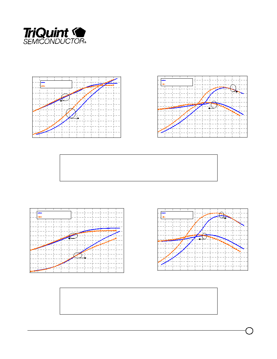
Power tuned data at 10GHz
Efficiency tuned data at 10GHz
For power tuned devices at 10GHz
Input matched for maximum gain & output load is:
Vd=12V, Idq=45mA: Rp = 57.0
, Cp = 0.257pF,
= 0.400,
= 104.7�
Vd=10V, Idq=75mA: Rp = 44.6
, Cp = 0.276pF,
= 0.382,
= 120.1�
For efficiency tuned devices at 10GHz:
Input matched for maximum gain & output load is:
Vd=12V, Idq=45mA: Rp = 74.2
, Cp = 0.255pF,
= 0.466,
= 93.4�
Vd=10V, Idq=45mA: Rp = 72.5
, Cp = 0.252pF,
= 0.455,
= 93.7�
5
6
7
8
9
10
11
12
13
14
15
16
17
18
19
8
9
10
11
12
13
14
15
16
17
18
19
20
Input Power (dBm)
Ga
in (
d
B)
10
14
18
22
26
30
34
38
42
46
50
54
58
62
PA
E (%
)
Vd = 12V, Id = 45mA
Vd = 10V, Id = 45mA
5
6
7
8
9
10
11
12
13
14
15
16
17
18
19
8
9
10
11
12
13
14
15
16
17
18
19
20
Input Power (dBm)
G
a
in (
d
B)
10
14
18
22
26
30
34
38
42
46
50
54
58
62
PA
E (%)
Vd = 12V, Id = 45mA
Vd = 10V, Id = 45mA
10
12
14
16
18
20
22
24
26
28
30
32
8
9
10
11
12
13
14
15
16
17
18
19
20
Input Power (dBm)
P
out
(
dBm
)
50
60
70
80
90
100
110
120
130
140
150
Id (
m
A)
Vd = 12V, Id = 45mA
Vd = 10V, Id = 45mA
10
12
14
16
18
20
22
24
26
28
30
32
34
36
38
8
9
10
11
12
13
14
15
16
17
18
19
20
Input Power (dBm)
Pout
(
d
B
m
)
50
60
70
80
90
100
110
120
130
140
150
160
170
180
Id
(m
A)
Vd = 12V, Id = 45mA
Vd = 10V, Id = 45mA


