TriQuint Semiconductor Texas : (972)994 8465 Fax: (972)994 8504 Web: www.triquint.com
Product Data Sheet
December 16, 2002
1
DC - 12 GHz Discrete HFET TGF4230-SCC
Key Features and Performance
∑
Nominal Pout of 28.5 dBm at 8.5 GHz
∑
Nominal Gain of 10.0 dB at 8.5 GHz
∑
Nominal PAE of 55 % at 8.5 GHz
∑
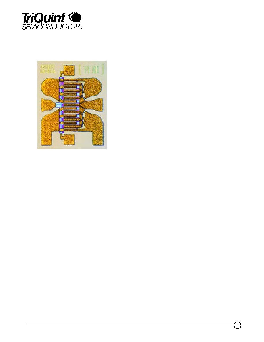
1200 µm HFET
∑
0.61 x 0.74 x 0.1 mm (0.024 x 0.029 x
0.004 in)
∑
Bias at 8 Volts, 96 mA
Description
The TriQuint TGF4230-SCC is a single gate 1.2 mm Discrete GaAs Heterostructure Field
Effect Transistor (HFET) designed for high-efficiency power applications up to 12 GHz in
Class A and Class AB operation.
Bond-pad and backside metalization is gold plated for compatibility with eutectic alloy
attach methods as well as thermocompression and thermosonic wire-bonding processes.
The TGF4230-SCC is readily assembled using automatic equipment.
For an Application Note on the use of HFETs, refer to the TriQuint website for the
Millimeter Wave Division.
Primary Applications
∑
Cellular Base Stations
∑
High dynamic-range LNAs
∑
Military and Space

TriQuint Semiconductor Texas : (972)994 8465 Fax: (972)994 8504 Web: www.triquint.com
Product Data Sheet
December 16, 2002
2
TABLE I
MAXIMUM RATINGS
SYMBOL
PARAMETER 1/
VALUE
NOTES
V
DS
Drain to Source Voltage
12 V
V
GS
Gate to Source Voltage Range
0 to -5.0 Volts
P
D
Power Dissipation
See Thermal Data
T
CH
Operating Channel Temperature
150
∞C
2/, 3/
T
STG
Storage Temperature
-65 to 150
∞C
T
M
Mounting Temperature (30 seconds)
320
∞C
1/ These ratings represent the maximum values for this device. Stresses beyond those listed
under "Maximum Ratings" may cause permanent damage to the device. These are stress
ratings only, and functional operation of the device at these or any other conditions beyond
those indicated under "DC Probe Characteristics" and "Electrical Characteristics" is not
implied. Exposure to maximum rated conditions for extended periods may affect device
reliability.
2/ Junction temperature will directly affect the device Mean Time to Failure (MTTF). For
maximum life, it is recommended that junction temperatures be maintained at the
lowest possible levels.
3/ These ratings apply to each individual FET
TGF4230-SCC

TriQuint Semiconductor Texas : (972)994 8465 Fax: (972)994 8504 Web: www.triquint.com
Product Data Sheet
December 16, 2002
3
TGF4230-SCC
TABLE II
DC PROBE CHARACTERISTICS
(T
A
= 25
∞C, Nominal)
Symbol
Parameter
Minimum
Typical
Maximum
Unit
Note
I
DSS
Saturated Drain Current
--
294
--
mA
1/
G
M
Transconductance
--
198
--
mS
1/
V
P
Pinch-off Voltage
1
1.85
3
V
2/
V
BGS
Breakdown Voltage
Gate-Source
17
22
30
V
2/
V
BGD
Breakdown Voltage
Gate-Drain
17
22
30
V
2/
1/ Total for two FETS
2/ V
P
, V
BGS
, and V
BGD
are negative.
T A B L E III
E L E C T R IC A L C H A R A C T E R IS T IC S
( T
A
= 2 5
∞C , N o m in a l)
B ia s C o n d itio n s : V d = 8 V , Id = 5 0 m A + /- 1 0 % , @ 8 .5 G H z
S y m b o l
P a r a m e t e r
T y p ic a l
U n it
P o u t
O u tp u t P o w e r
2 8 .5
d B m
G p
P o w e r G a in
1 0
d B
P A E
P o w e r A d d e d E ffic ie n c y
5 5
%
Note: The recommended bias current for HFETs is 80 mA/mm. For this
1.2 mm HFET IQ is 96 mA.

TriQuint Semiconductor Texas : (972)994 8465 Fax: (972)994 8504 Web: www.triquint.com
Product Data Sheet
December 16, 2002
4
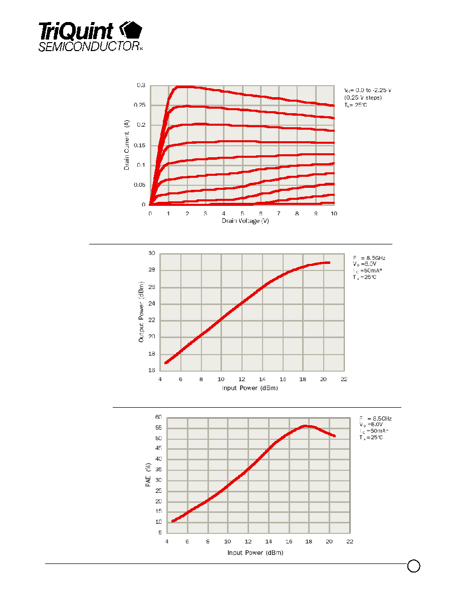
EXAMPLE OF
DC I-V CURVES
OUTPUT POWER VS.
INPUT POWER
POWER ADDED
EFFICIENCY VS.
INPUT POWER
TGF4230-SCC
TYPICAL PERFORMANCE

TriQuint Semiconductor Texas : (972)994 8465 Fax: (972)994 8504 Web: www.triquint.com
Product Data Sheet
December 16, 2002
5
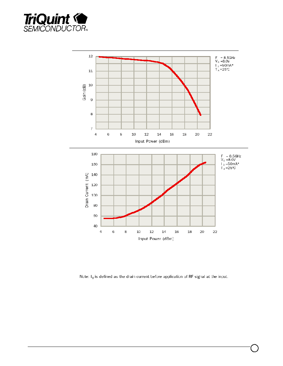
GAIN VS.
INPUT POWER
DRAIN CURRENT
VS. INPUT POWER
TGF4230-SCC
TYPICAL PERFORMANCE
*
