TriQuint Semiconductor Texas : (972)994 8465 Fax: (972)994 8504 Web: www.triquint.com
Product Data Sheet
March 31, 2003
1
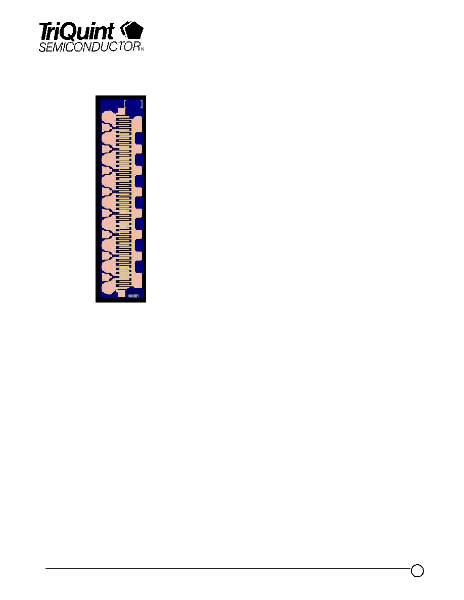
9.6 mm Discrete HFET TGF4260-SCC
Key Features and Performance
∑
9600 µm x 0.5 µm HFET
∑
Nominal Pout of 37dBm at 6 GHz
∑
Nominal Gain of 9.5dB at 6 GHz
∑
Nominal PAE of 52% at 6 GHz
∑
Frequency Range: DC - 10.5 GHz
∑
Suitable for high reliability applications
∑
0.6 x 2.4 x 0.1 mm (0.024 x 0.093 x 0.004 in)
Description
The TriQuint TGF4260-SCC is a single gate 9.6 mm discrete GaAs Heterostructure
Field Effect Transistor (HFET) designed for high efficiency power applications up to
10.5 GHz in Class A and Class AB operation.
Typical performance at 6 GHz is 37dBm power output, 9.5 dB Gain, and 52% PAE.
Bond pad and backside metallization are gold plated for compatibility with eutectic
alloy attach methods as well as thermocompression and thermosonic wire bonding
processes.
The TGF4260-SCC is readily assembled using automatic equipment.
Primary Applications
∑
Cellular Base Stations
∑
High-reliability space
∑
Military

TriQuint Semiconductor Texas : (972)994 8465 Fax: (972)994 8504 Web: www.triquint.com
Product Data Sheet
March 31, 2003
2
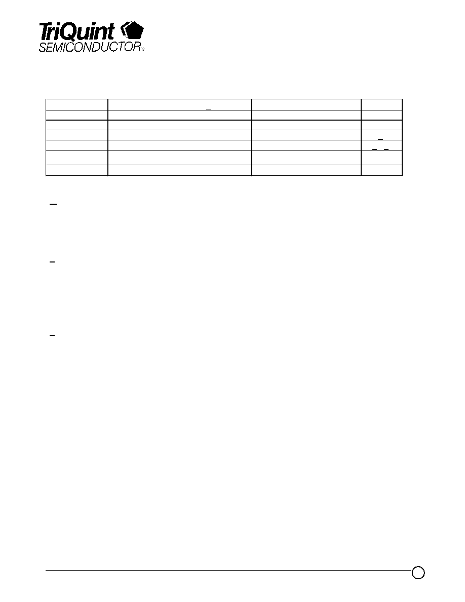
TABLE I
MAXIMUM RATINGS
SYMBOL
PARAMETER 1/
VALUE
NOTES
V
DS
Drain to Source Voltage
12 V
V
GS
Gate to Source Voltage Range
0 to -5.0 Volts
P
D
Power Dissipation
6.8 W
2/
T
CH
Operating Channel Temperature
150
∞C
3/, 4/
T
STG
Storage Temperature
-65 to 200
∞C
T
M
Mounting Temperature (30 seconds)
320
∞C
1/ These ratings represent the maximum values for this device. Stresses beyond those listed
under "Maximum Ratings" may cause permanent damage to the device. These are stress
ratings only, and functional operation of the device at these or any other conditions beyond
those indicated under "DC Probe Characteristics" is not implied. Exposure to maximum rated
conditions for extended periods may affect device reliability.
2/ When operated at this bias condition with a base plate temperature of 70
0
C, the MTTF life is
reduced from 1.7 E+12 to 3 E+9 hours.
3/ Junction temperature will directly affect the device Mean Time to Failure (MTTF). For
maximum life, it is recommended that junction temperatures be maintained at the
lowest possible levels
4/ These ratings apply to each individual FET
TGF4260-SCC

TriQuint Semiconductor Texas : (972)994 8465 Fax: (972)994 8504 Web: www.triquint.com
Product Data Sheet
March 31, 2003
3
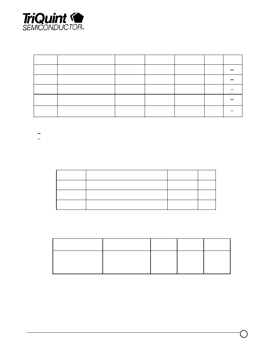
TABLE II
DC PROBE CHARACTERISTICS
(T
A
= 25
∞C, Nominal)
Symbol
Parameter
Minimum
Typical
Maximum
Unit
Note
I
DSS
Saturated Drain Current
--
2352
--
mA
1/
G
M
Transconductance
--
1584
--
mS
1/
V
P
Pinch-off Voltage
1
1.85
3
V
2/
V
BGS
Breakdown Voltage
Gate-Source
17
22
30
V
2/
V
BGD
Breakdown Voltage
Gate-Drain
17
22
30
V
2/
1/ Total for eight FETS
2/ V
P
, V
BGS
, and V
BGD
are negative.
TABLE III
ELECTRICAL CHARACTERISTICS
(T
A
= 25
∞C, Nominal)
Bias Conditions: Vd = 8.5 V, Id = 520 mA
Symbol
Parameter
Typical
Unit
Pout
Output Power
37
dBm
Gp
Power Gain
9.5
dB
PAE
Power Added Efficiency
52
%
TGF4260-SCC
TABLE IV
THERMAL INFORMATION*
Parameter
Test Conditions
T
CH
(
o
C)
R
qJC
(
∞C/W)
T
M
(HRS)
R
qJC
Thermal
Resistance
(channel to backside
of carrier)
Vd = 8.5 V
I
D
= 520 mA
Pdiss = 6.8 W
101.64
7.16
1.7 E+12
Note: Assumes eutectic attach using 1.5 mil 80/20 AuSn mounted to a 20 mil
CuMo Carrier at 70
∞C baseplate temperature. Worst case condition with no RF
applied, 100% of DC power is dissipated.
* The thermal information is a result of a detailed thermal model.

TriQuint Semiconductor Texas : (972)994 8465 Fax: (972)994 8504 Web: www.triquint.com
Product Data Sheet
March 31, 2003
4
TGF4260-SCC
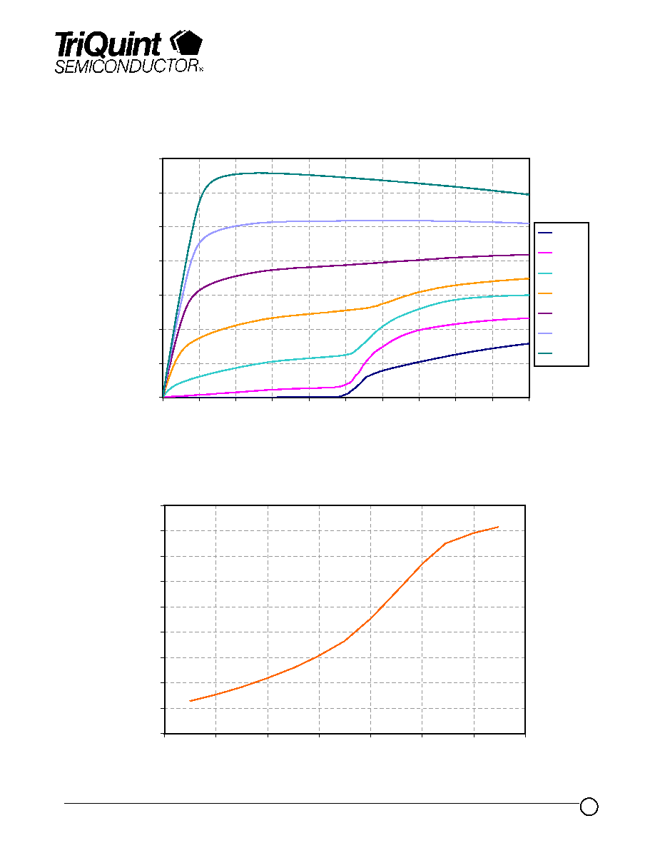
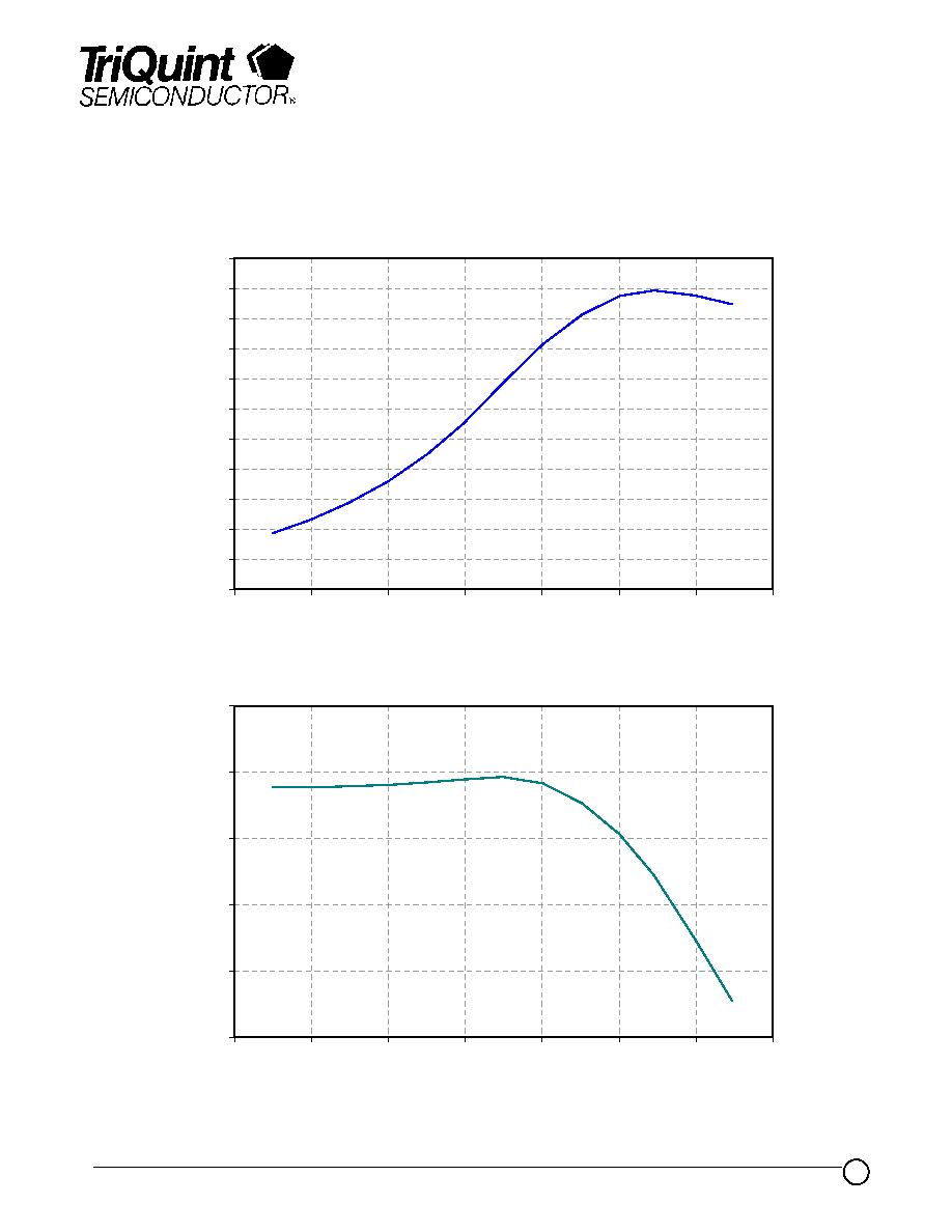
TYPICAL PERFORMANCE
(T
A
= 25
∞C, Nominal)
Bias Conditions: F = 6 GHz, Vd = 8.5 V, Iq = 795 mA
0.8
0.85
0.9
0.95
1
1.05
1.1
1.15
1.2
1.25
16
18
20
22
24
26
28
30
Input Power (dBm)
Dr
ain
Cu
r
r
e
n
t
(A)
0.0
0.2
0.4
0.6
0.8
1.0
1.2
1.4
0
1
2
3
4
5
6
7
8
9
10
Drain Voltage (V)
Dra
i
n Curre
nt (A)
-2.25 V
-2.0 V
-1.75 V
-1.5 V
-1.25 V
-1.0 V
-0.75 V
Vg

TriQuint Semiconductor Texas : (972)994 8465 Fax: (972)994 8504 Web: www.triquint.com
Product Data Sheet
March 31, 2003
5
TGF4260-SCC
TYPICAL PERFORMANCE
8
9
10
11
12
13
16
18
20
22
24
26
28
30
Input Power (dBm)
Gain (dB)
0
5
10
15
20
25
30
35
40
45
50
55
16
18
20
22
24
26
28
30
Input Power (dBm)
PAE (
%
)
Bias Conditions: F = 6 GHz, Vd = 8.5 V, Iq = 795 mA
