 | –≠–ª–µ–∫—Ç—Ä–æ–Ω–Ω—ã–π –∫–æ–º–ø–æ–Ω–µ–Ω—Ç: TGP6336 | –°–∫–∞—á–∞—Ç—å:  PDF PDF  ZIP ZIP |

TriQuint Semiconductor Texas Phone: (972)994 8465 Fax: (972)994 8504 Web: www.triquint.com
Product Data Sheet
1
6 - 18 GHz Phase Shifter TGP6336-EEU
Key Features and Performance
∑
6 to 18 GHz Frequency Range
∑
5-Bit Phase Shifter
∑
On-Chip CMOS-Compatible Drivers
∑
9 dB Typical Insertion Loss at Midband
∑
2:1 Typical Input SWR: 2.6:1 Typical
Output SWR
∑
3.556 x 2.540 x 0.1016 mm (0.140 x
0.100 x 0.004 in.)
Description
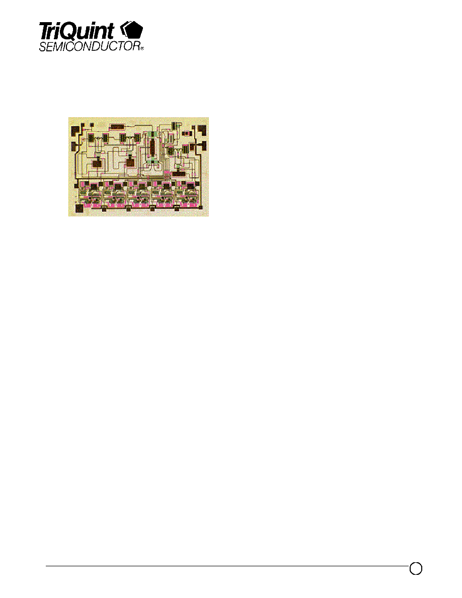
The TriQuint TGP6336-EEU is a GaAs MMIC 5-bit phase shifter which operates
from 6 to 18 GHz. Phase can be shifted from 0 to 348.75 degrees in 11.25 degree
steps. Control bias voltages are 0 and 5 V. The insertion loss is typically 9 dB.
The TGP6336-EEU features on-chip CMOS-compatible drivers. The FET based
phase shifter offers wide band performance and small size for use in T/R modules
for EW applications.
Bond pad and backside metallization is gold plated for compatibility with eutectic
alloy attach methods as well as thermocompression and thermosonic wire-bonding
processes. Ground is provided to the circuitry through vias to the backside
metallization.

TriQuint Semiconductor Texas Phone: (972)994 8465 Fax: (972)994 8504 Web: www.triquint.com
Product Data Sheet
2
TGP6336-EEU
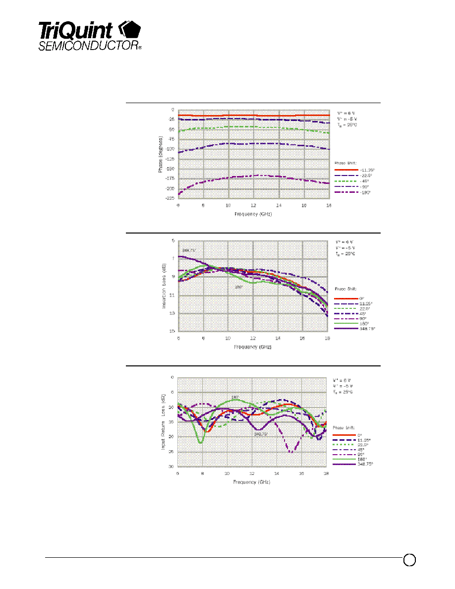
TYPICAL
INPUT
RETURN LOSS
TYPICAL
RELATIVE
PHASE
TYPICAL
INSERTION
LOSS

TriQuint Semiconductor Texas Phone: (972)994 8465 Fax: (972)994 8504 Web: www.triquint.com
Product Data Sheet
3
TGP6336-EEU
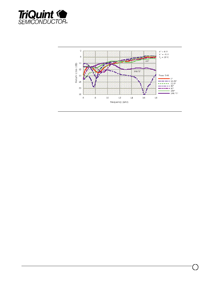
ABSOLUTE
MAXIMUM
RATINGS
TYPICAL OUTPUT
RETURN LOSS
Positive supply voltage, V+............................................................................................... 8 V
Positive supply voltage range w ith respect to negative supply voltage, V+ - V-............................ 0 V to 12 V
Negative supply voltage range, V-...................................................................................... 0 V to -6 V
Input continuous w ave pow er, P
IN
.......................................................................................1 W
Control voltage range, SHF 90, SHF180, SHF11.25, SHF 22.5, SHF 45...................................... 0 V to V+
Operating Channel temperature, T
CH
*..................................................................................150
o
C
Mounting temperature (30 sec.), T
M
.....................................................................................320
o
C
Storage temperature range, T
STG
........................................................................................-65 to 150
o
C
Ratings over operating channel temperature range, T
CH
(unless otherw ise noted).
Stresses beyond those listed under "Absolute Maximum Ratings" may cause permanent damage to the device.
These are stress ratings only, and functional operation of the device at these or any other conditions beyond
those indicated under "RF Characteristics" is not implied. Exposure to absolute maximum rated conditions
for extended periods may affect device reliability.
* Operating channel temperature (T
CH
) w ill directly affect the device MTTF. For maximum life, it is recommended
that channel temperature be maintained at the low est possible level.

TriQuint Semiconductor Texas Phone: (972)994 8465 Fax: (972)994 8504 Web: www.triquint.com
Product Data Sheet
4
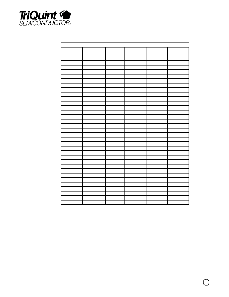
BIAS TRUTH TABLE
TGP6336-EEU
V+ = 6 V, V- = -5 V, T
A
= 25
o
C
RELATIVE
SHF 180
SHF 90
SHF 45
SHF 22.5
SHF 11.25
PHASE SHIFT (Bond pad #10) (Bond pad #11 (Bond pad #7) (Bond pad #8) (Bond pad #9)
(degrees)
0.00
5
5
5
5
5
-11.25
5
5
5
5
0
-22.50
5
5
5
0
5
-33.75
5
5
5
0
0
-45.00
5
5
0
5
5
-56.25
5
5
0
5
0
-67.50
5
5
0
0
5
-78.75
5
5
0
0
0
-90.00
5
0
5
5
5
-101.25
5
0
5
5
0
-112.50
5
0
5
0
5
-123.75
5
0
5
0
0
-135.00
5
0
0
5
5
-146.25
5
0
0
5
0
-157.50
5
0
0
0
5
-168.75
5
0
0
0
0
-180.00
0
5
5
5
5
-191.25
0
5
5
5
0
-202.50
0
5
5
0
5
-213.75
0
5
5
0
0
-225.00
0
5
0
5
5
-236.25
0
5
0
5
0
-247.50
0
5
0
0
5
-258.75
0
5
0
0
0
-270.00
0
0
5
5
5
-281.25
0
0
5
5
0
-292.50
0
0
5
0
5
-303.75
0
0
5
0
0
-315.00
0
0
0
5
5
-326.25
0
0
0
5
0
-337.50
0
0
0
0
5
-348.75
0
0
0
0
0

TriQuint Semiconductor Texas Phone: (972)994 8465 Fax: (972)994 8504 Web: www.triquint.com
Product Data Sheet
5
TGP6336-EEU
RF CHARACTERISTICS
RECOMMENDED BIAS
NETWORK
V+ = 6 V, V- = -5 V, T
A
= 25
o
C
All bias resistors have a nominal value of 25-Ohms.
RF connections: Bond one 1-mil diameter, 20 to 25-mil-length gold bond wires at both RF Input and
RF Output for optimum RF performance.
Close placement of external components is essential for resonant-free performance.
Refer to TriQuint's Gallium Arsenide Products Designers' Information on our website under Application
Information.
PARAMETER
TEST CONDITIONS
TYP
UNIT
IL
Insertion loss (all states)
f = 6 - 18 GHz
9
dB
SWR(in)
Input standing w ave ratio
f = 6 - 18 GHz (all states)
2.0:1
-
SWR(out) Output standing w ave ratio
f = 6 - 18 GHz (all states)
2.6:1
-
P
1dB
(in)
Input pow er at 1≠dB gain compression
see next table
PHASE
TYPICAL RELATIVE PHASE SHIFT
TYPICAL INPUT POWER at
SHIFT
at 6GHz
at 12GHz
at 18GHz
1≠dB GAIN COMPRESSION at
(degrees)
(degrees)
(degrees)
(degrees)
MIDBAND(dBm)
-11.25
-13±2
-13.5±2
13±4
26
-22.5
-23±2
-23±2
32±4
27
-45
-55±4
-43±3
58±7
26
-90
-107±5
-84±7
99±8
25
-180
-214±4
-165±8
186±16
25
-348.75
-416±8
-326±9
380±11
25

TriQuint Semiconductor Texas Phone: (972)994 8465 Fax: (972)994 8504 Web: www.triquint.com
Product Data Sheet
6
TGP6336-EEU
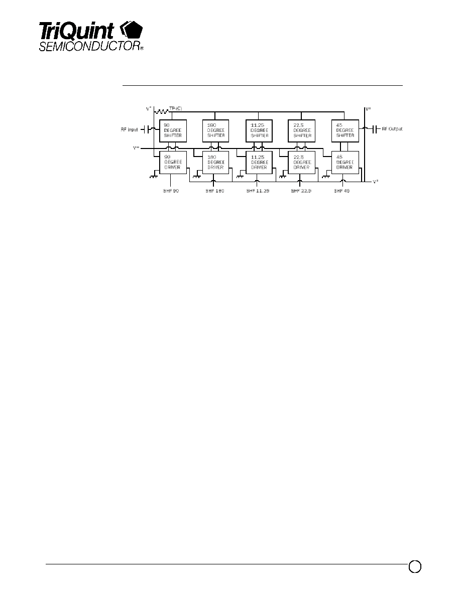
FUNCTIONAL BLOCK
DIAGRAM

TriQuint Semiconductor Texas Phone: (972)994 8465 Fax: (972)994 8504 Web: www.triquint.com
Product Data Sheet
7
TGP6336-EEU
GaAs MMIC devices are susceptible to damage from Electrostatic Discharge. Proper precautions should be observed
during handling, assembly and test.
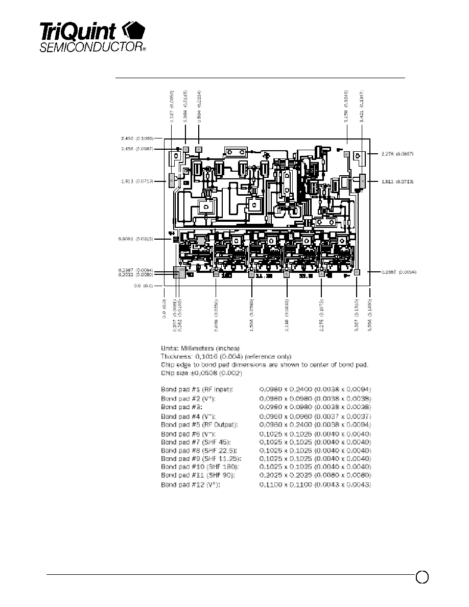
MECHANICAL
DRAWING
