TriQuint Semiconductor Texas: Phone (972)994-8465 Fax (972)994-8504 Email: Info-mmw@tqs.com Web: www.triquint.com
Advance Product Information
July 22, 2004
1
77 GHz Transceiver Switch
Key Features
∑
I/O Compatible with MA4GC6772
∑
3 Antenna Ports
∑
Receive, Source, and LO Ports
∑
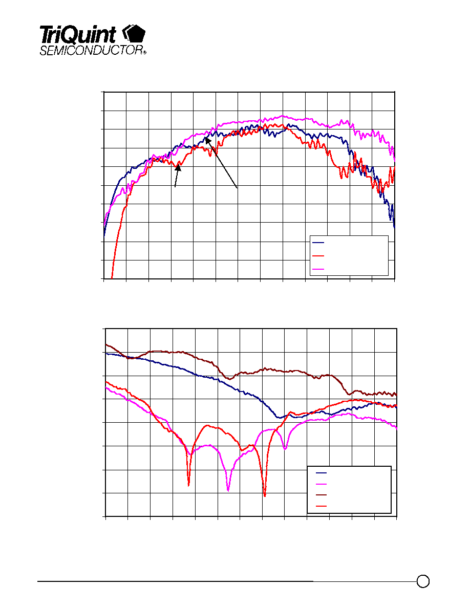
2.5 dB RX/TX Insertion Loss Typical
∑
40 dB Source/Mixer Isolation Typical
∑
25 dB Ant/Ant Isolation Typical
∑
Bias Supply: 1.3V@40mA
∑
Die Size: 1.70 x 2.16 x 0.1 mm
Primary Applications
∑
Automotive Radar
∑
Instrumentation
Note: Devices designated as EPU are typically early in their characterization process prior to finalizing all electrical and process specifications.
Specifications are subject to change without notice
TGS4307-EPU
Product Description
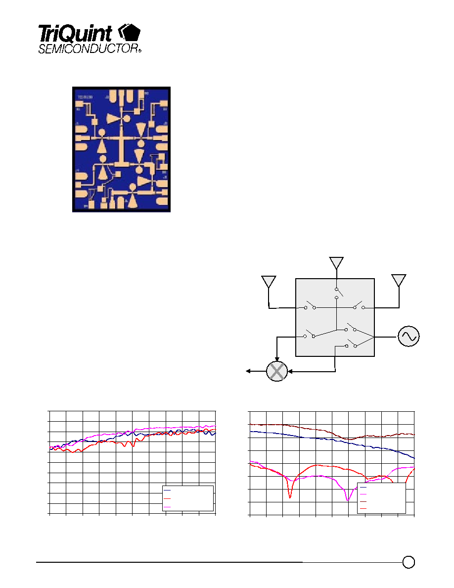
The TGS4307 is a 77 GHz switch matrix for
use in automotive radar transceivers. The
switch is designed using TriQuint's proven
VPIN diode production process.
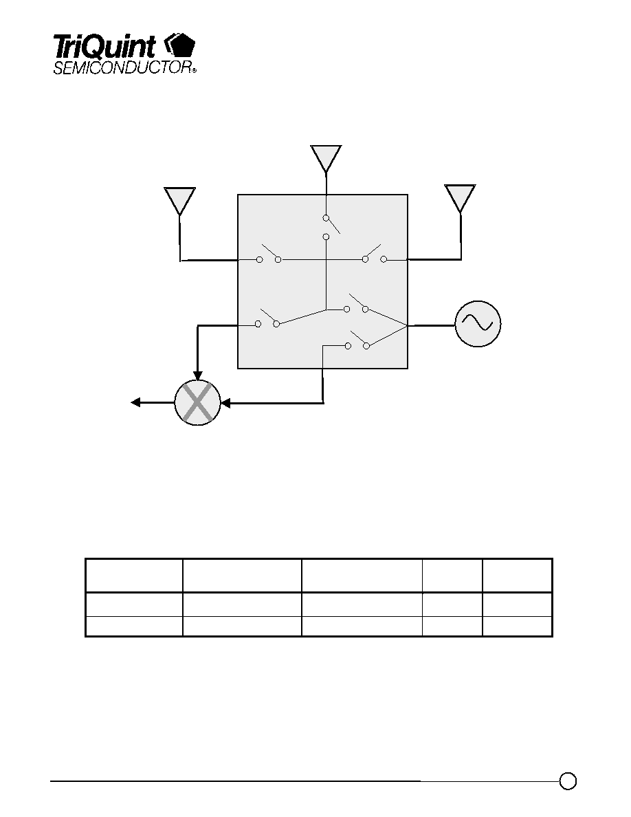
Three antenna ports may be selected
independently and directed to a source (J5)
or a receive (J4) port. Additionally, the
source port can be directed to the LO port
for use with a downconverting mixer.
Measured Fixtured Data
Bias: 1.3V @ 40mA
Radar Application Schematic
-10
-9
-8
-7
-6
-5
-4
-3
-2
-1
0
70
71
72
73
74
75
76
77
78
79
80
Frequency (GHz)
I
n
s
e
r
t
i
on
Los
s
(
d
B)
Receive Path
Transmit Path
LO Path
-80
-70
-60
-50
-40
-30
-20
-10
0
70
71
72
73
74
75
76
77
78
79
80
Frequency (GHz)
Is
o
l
a
t
io
n
(
d
B)
Ant / Ant
Source / Ant
Source / LO
Source / RX
J1
TGS4307
J3
J2
J6
IF
J5
J4
RX Port
Source
Port
LO Port
B1
B3
B2
B4
B5
B4

TriQuint Semiconductor Texas: Phone (972)994-8465 Fax (972)994-8504 Email: Info-mmw@tqs.com Web: www.triquint.com
Advance Product Information
July 22, 2004
2
TABLE I
MAXIMUM RATINGS
1/
SYMBOL
PARAMETER
VALUE
NOTES
V
+
Positive Supply Voltage
2 V
2/
V
-
Negative Supply Voltage
-8 V
2/
I
+
Positive Supply Current (Quiescent)
80 mA
2/, 3/
P
IN
Input Continuous Wave Power
TBD
P
D
Power Dissipation
160 mW
2/
T
M
Mounting Temperature (30 Seconds)
320
0
C
T
STG
Storage Temperature
-65 to 150
0
C
1/
These ratings represent the maximum operable values for this device.
2/
Combinations of supply voltage, supply current, input power, and output power shall not exceed P
D
.
3/
Control line B1, B2, B3 maximum current = 20 mA
Control line B4, B5 maximum current = 40 mA
TGS4307-EPU
Note: Devices designated as EPU are typically early in their characterization process prior to finalizing all electrical and process specifications.
Specifications are subject to change without notice
P A R A M E T E R
TY P IC A L
U N ITS
Frequency R ange
75 - 80
G H z
B ias Supply
1.3V @ 40m A
Insertion Loss, P ort J3 to J4 (R X )
2.5
dB
Insertion Loss, P ort J1 to J5 (TX )
2.5
dB
Insertion Loss S ource to LO , P ort J5 to J6 (R X)
1.8
dB
Isolation S ource to R X , Port J4 to J5 (R X )
> 40
dB
Isolation S ource to A ntenna, P ort J1 to J5 (R X )
> 40
dB
Isolation A ntenna to A ntenna, P ort J1 to J3 (R X ,TX )
25
dB
Isolation S ource to LO , P ort J5 to J6 (TX )
20
dB
R eturn Loss
>8
dB
TABLE II
ELECTRICAL CHARACTERISTICS
(Ta = 25
0
C Nominal)

TriQuint Semiconductor Texas: Phone (972)994-8465 Fax (972)994-8504 Email: Info-mmw@tqs.com Web: www.triquint.com
Advance Product Information
July 22, 2004
3
TGS4307-EPU
Preliminary Measured Data
Bias: 1.3V @ 40mA
Note: Devices designated as EPU are typically early in their characterization process prior to finalizing all electrical and process specifications.
Specifications are subject to change without notice
-10
-9
-8
-7
-6
-5
-4
-3
-2
-1
0
65
67
69
71
73
75
77
79
81
83
85
87
89
91
Frequency (GHz)
Ins
e
r
t
ion
Los
s
(
d
B
)
Receive Path
Transmit Path
LO Path
-80
-70
-60
-50
-40
-30
-20
-10
0
65
67
69
71
73
75
77
79
81
83
85
87
89
91
Frequency (GHz)
Is
ola
t
ion (
d
B
)
Ant / Ant
Source / Ant
Source / LO
Source / RX
Ant/Ant
Source/LO
Source/RX
Source/Ant
LO Path
Receive Path
Transmit Path

TriQuint Semiconductor Texas: Phone (972)994-8465 Fax (972)994-8504 Email: Info-mmw@tqs.com Web: www.triquint.com
Advance Product Information
July 22, 2004
4
Note: Devices designated as EPU are typically early in their characterization process prior to finalizing all electrical and process specifications.
Specifications are subject to change without notice
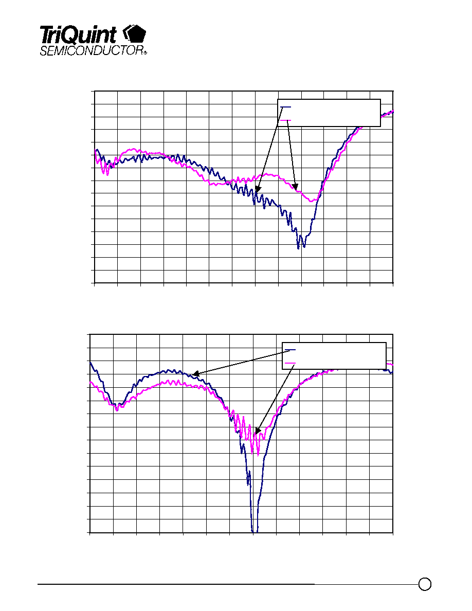
Preliminary Measured Data
-30
-28
-26
-24
-22
-20
-18
-16
-14
-12
-10
-8
-6
-4
-2
0
65
67
69
71
73
75
77
79
81
83
85
87
89
91
Frequency (GHz)
R
e
tu
r
n
L
o
s
s
(d
B
)
RL @ RX Port
RL @ Antenna Port
Antenna 3 to RX Port
-30
-28
-26
-24
-22
-20
-18
-16
-14
-12
-10
-8
-6
-4
-2
0
65
67
69
71
73
75
77
79
81
83
85
87
89
91
Frequency (GHz)
R
e
t
u
r
n
Loss
(
d
B
)
RL @ Antenna Port
RL @ Source Port
Source Port to Antenna 1
TGS4307-EPU

TriQuint Semiconductor Texas: Phone (972)994-8465 Fax (972)994-8504 Email: Info-mmw@tqs.com Web: www.triquint.com
Advance Product Information
July 22, 2004
5
TGS4307-EPU
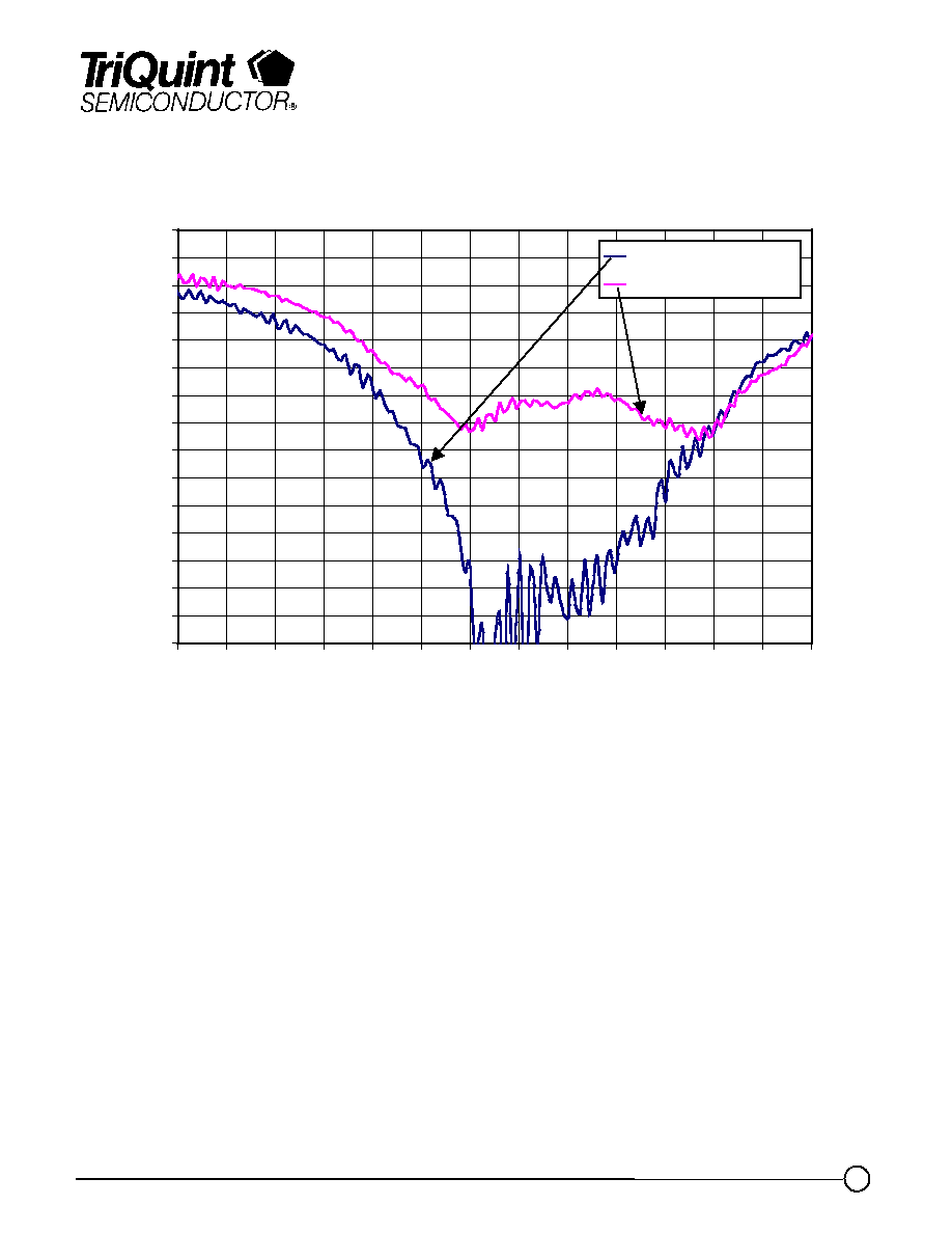
Preliminary Measured Data
Source Port to LO Port
-30
-28
-26
-24
-22
-20
-18
-16
-14
-12
-10
-8
-6
-4
-2
0
65
67
69
71
73
75
77
79
81
83
85
87
89
91
Frequency (GHz)
R
e
t
u
r
n
Loss
(
d
B
)
RL @ LO Port
RL @ Source Port
Note: Devices designated as EPU are typically early in their characterization process prior to finalizing all electrical and process specifications.
Specifications are subject to change without notice

TriQuint Semiconductor Texas: Phone (972)994-8465 Fax (972)994-8504 Email: Info-mmw@tqs.com Web: www.triquint.com
Advance Product Information
July 22, 2004
6
Mechanical Drawing
GaAs MMIC devices are susceptible to damage from Electrostatic Discharge. Proper precautions should
be observed during handling, assembly and test.
Note: Devices designated as EPU are typically early in their characterization process prior to finalizing all electrical and process specifications.
Specifications are subject to change without notice
TGS4307-EPU
1
2
3
4
5
6
7
8
9
10
11
0
0
0.103
(0.004)
0.341
(0.013)
0.717
(0.028)
1.657
(0.065)
1.760
(0.069)
0.103
(0.004)
0.335
(0.013)
0.775
(0.031)
1.274
(0.050)
1.873
(0.074)
2.038
(0.080)
1.638
(0.064)
1.230
(0.048)
0.880
(0.035)
0.123
(0.005)
2.160
(0.085)
2.058
(0.081)
1.870
(0.074)
1.274
(0.050)
0.463
(0.018)
0.123
(0.005)
Units: millimeters (inches)
Thickness: 0.1016 (0.004)
Chip edge to bond pad dimensions are shown to center of bond pads
Chip size tolerance: +/- 0.05 (0.002)
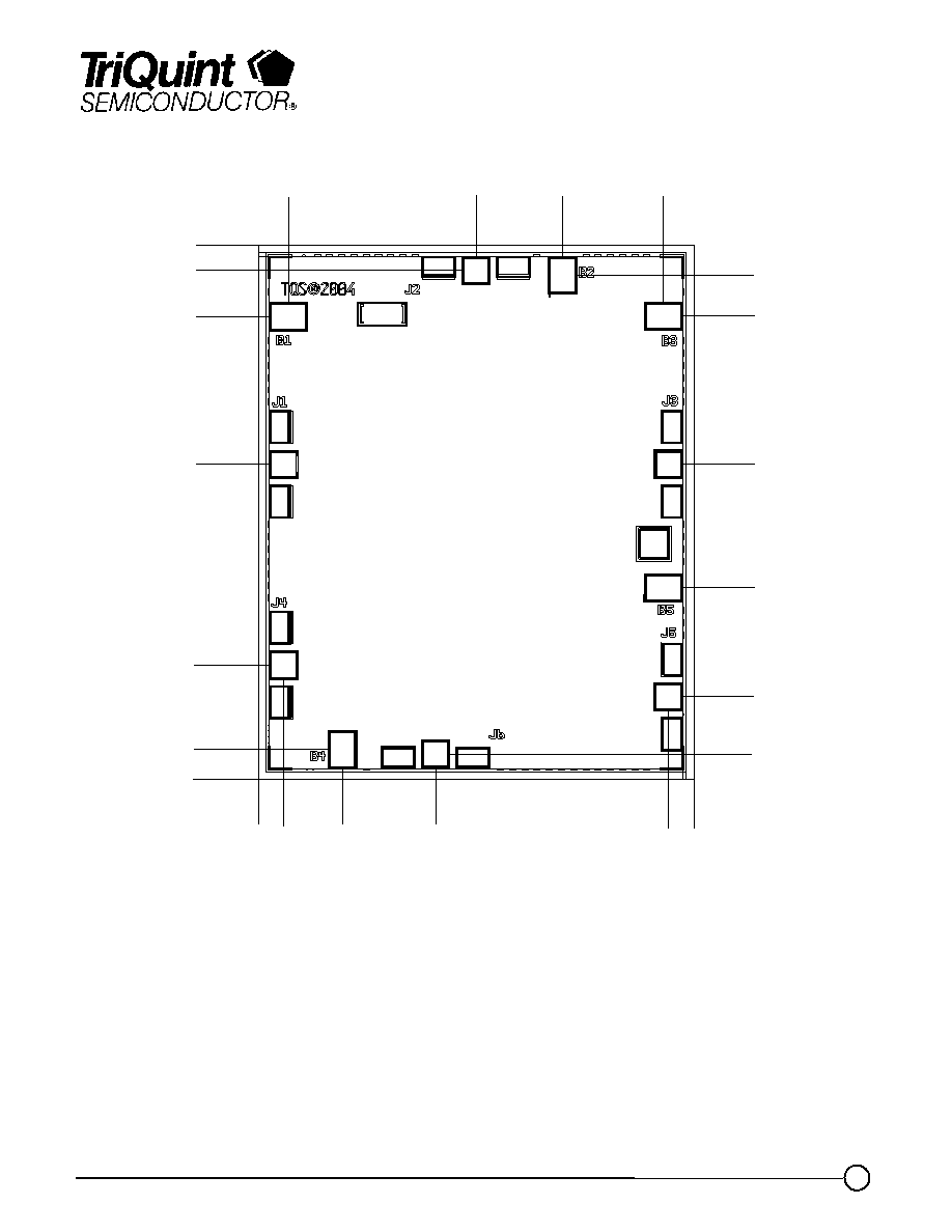
GND IS BACKSIDE OF MMIC
Bond Pad # 1 (Antenna Port 1)
Bond Pad # 2 (VB1)
Bond Pad # 3 (Antenna Port 2)
Bond Pad # 4 (VB2)
Bond Pad # 5 (VB3)
Bond Pad # 6 (Antenna Port 3)
Bond Pad # 7 (VB5)
Bond Pad # 8 (Source Port)
Bond Pad # 9 (LO Port)
Bond Pad # 10 (VB4)
Bond Pad # 11 (Receiver Port)
0.100 x 0.100 (0.004 x 0.004)
0.140 x 0.100 (0.006 x 0.004)
0.100 x 0.100 (0.004 x 0.004)
0.100 x 0.140 (0.004 x 0.006)
0.140 x 0.100 (0.006 x 0.004)
0.100 x 0.100 (0.004 x 0.004)
0.140 x 0.100 (0.006 x 0.004)
0.100 x 0.100 (0.004 x 0.004)
0.100 x 0.100 (0.004 x 0.004)
0.100 x 0.140 (0.004 x 0.006)
0.100 x 0.100 (0.004 x 0.004)

TriQuint Semiconductor Texas: Phone (972)994-8465 Fax (972)994-8504 Email: Info-mmw@tqs.com Web: www.triquint.com
Advance Product Information
July 22, 2004
7
TGS4307-EPU
Assembly Drawing
GaAs MMIC devices are susceptible to damage from Electrostatic Discharge. Proper precautions should
be observed during handling, assembly and test.
Note: Devices designated as EPU are typically early in their characterization process prior to finalizing all electrical and process specifications.
Specifications are subject to change without notice
B1
B2
B3
B4
B5
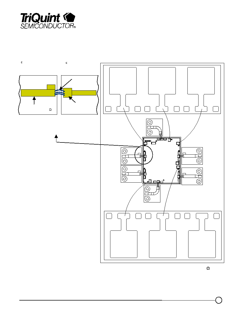
Note: Unused Ports should be terminated with 50 .
Substrate: GaAs
r
=12.9
Thickness=4mil
Note: Ribbon bond is acceptable
(instead of 3 bondwires)
Recommended Interconnect Scheme
Substrate: Alumina
r
=9.8
Thickness=5mil
External Interface (TFN)
Switch MMIC
Microstrip Trace
Width=120mm (50 )
3 Bondwires
Gap ~4mil
Diameter=0.7mil
Height< 1mil
5mil
3mil
RF I/O Pad
TFN

TriQuint Semiconductor Texas: Phone (972)994-8465 Fax (972)994-8504 Email: Info-mmw@tqs.com Web: www.triquint.com
Advance Product Information
July 22, 2004
8
Function
Selected Antenna
(B1, B2, or B3)
Unused Antennas
(B1, B2, or B3)
B4
B5
Transmit
-5 to 0V
+10mA each
+20mA
0V
Receive
-5 to 0V
+10mA each
0V
+20mA
Bias State Table
Forward voltage is ~ +1.3V to achieve bias current
Application Schematic
TGS4307-EPU
Note: Devices designated as EPU are typically early in their characterization process prior to finalizing all electrical and process specifications.
Specifications are subject to change without notice
GaAs MMIC devices are susceptible to damage from Electrostatic Discharge. Proper precautions should
be observed during handling, assembly and test.
J1
TGS4307
J3
J2
J6
IF
J5
J4
RX Port
Source
Port
LO Port
B1
B3
B2
B4
B5
B4

TriQuint Semiconductor Texas: Phone (972)994-8465 Fax (972)994-8504 Email: Info-mmw@tqs.com Web: www.triquint.com
Advance Product Information
July 22, 2004
9
Assembly Process Notes
GaAs MMIC devices are susceptible to damage from Electrostatic Discharge. Proper precautions should
be observed during handling, assembly and test.
TGS4307-EPU
Note: Devices designated as EPU are typically early in their characterization process prior to finalizing all electrical and process specifications.
Specifications are subject to change without notice
Reflow process assembly notes:
∑
Use AuSn (80/20) solder with limited exposure to temperatures at or above 300
0
C (30 seconds max).
∑
An alloy station or conveyor furnace with reducing atmosphere should be used.
∑
No fluxes should be utilized.
∑
Coefficient of thermal expansion matching is critical for long-term reliability.
∑
Devices must be stored in a dry nitrogen atmosphere.
Component placement and adhesive attachment assembly notes:
∑
Vacuum pencils and/or vacuum collets are the preferred method of pick up.
∑
Air bridges must be avoided during placement.
∑
The force impact is critical during auto placement.
∑
Organic attachment can be used in low-power applications.
∑
Curing should be done in a convection oven; proper exhaust is a safety concern.
∑
Microwave or radiant curing should not be used because of differential heating.
∑
Coefficient of thermal expansion matching is critical.
Interconnect process assembly notes:
∑
Wedge bonding is the preferred interconnect technique.
∑
Force, time, and ultrasonics are critical parameters.
∑
Aluminum wire should not be used.
∑
Maximum stage temperature is 200
0
C.
